Please read this page about taking my exams!
Exam format
- When/where
- Mon/Wed section: Tue 12/9 at 4:00 PM in the normal room (5502 SENSQ)
- Tue/Thu section: Thu 12/11 at 2:00 PM in the normal room (107 LAWRN)
- Closed-note, no calculator
- You may not have any notes, cheat sheets etc. to take the exam
- The math on the exam has been designed to be doable either in your head or very quickly on paper (e.g. 2 x 1 digit multiplication); if you find yourself needing a calculator, you did something wrong
- PUT numbers in scientific notation before you start
- KEEP numbers in scientific notation, do not take them out of it until the end
- Avoid division when you can - do reciprocal first, then multiply by that
- I literally design the test questions to be easy to do reciprocals
- Length
- LONGER, probably 8 or 9 pages? 60 questions?
- 110 minutes (1 hour 50 minutes)
- Topic point distribution
- I am PLANNING on:
- ~35% exam1 material
- ~40% exam2 material
- ~25% new material (since exam2)
- I am PLANNING on:
- Kinds of questions
- Very much like the midterms
- But like………. bigger and more difficult versions of some of those questions
Topics
Since this is a cumulative exam, anything from the first two exams is fair game. So open their study guides too:
The rest of this page is everything we covered since exam2. Not everything will be on the exam, but anything could be on the exam.
ISA design
- ISA (Instruction Set Architecture) is programmer’s software interface to control CPU hardware
- ISA abstracts the hardware design, so that same program can work on any implementation
- but if we want to build a piece of hardware, the ISA is going to place some requirements on it
- e.g. having 32 hardware registers to represent the 32 ISA registers
- or maybe only 31…
zeroisn’t a real register, right?
- or maybe only 31…
- ISA design is under tension between users (programmers) and implementers (hardware designers)
- programmers want more bits, more registers, more powerful instructions
- hardware designers want higher yields, which usually means smaller, simpler circuits
- but hardware designers must also work within physical limitations of propagation delay, heat, power, and process ability
- CISC vs. RISC
- CISC designs gave the programmers what they wanted
- “Complex Instruction Set Computer”
- was just “the way CPUs are designed” for decades before around 1980
- huge instruction sets (thousands or tens of thousands of instructions)
- complex, multi-step instructions for doing common programming tasks (e.g. searching for items in arrays, comparing strings, copying large blocks of data around, doing for-loops)
- this put a lot of complexity into the CPU circuitry, and complex circuits can’t go very fast.
- Then RISC designs came along and changed everything
- “Reduced Instruction Set Computer”
- around 1980, a number of different teams of people asked, “is all the complexity in our CPUs actually worthwhile?”
- they did surveys of existing programs written in those CISC ISAs, and found that the vast majority of the instructions provided by those ISAs were never even used
- most programs used a very small subset of the ISAs
- so, they designed RISC ISAs from the ground up to have very few instructions, and made those instrutions extremely simple one-step operations
- the result was a CPU that was easier to implement, used less circuitry, used less power, and ran way faster - which was very counterintuitive to the CPU design orthodoxy of the time!
- CISC designs gave the programmers what they wanted
- microarchitecture: actual physical implementation of an ISA
- microarchitecture is to ISA, as class is to interface
- ISA says what things the CPU should be able to do
- microarchitecture is an implementation which does those things
- as long as 2 CPUs implement the same ISA, they can run the same programs, even if microarchitectures are completely different
- not just different companies’ designs, but different designs from 1 company over time
Parts of the CPU
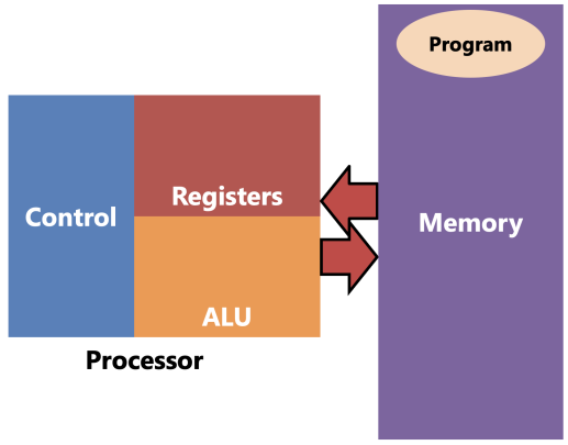
- Registers hold values being computed
- the register file has nothing to do with files on the hard drive. it contains the general-purpose registers
- it is essentially a small word-addressed memory with some special abilities (e.g. read from 2 places at once)
- the general-purpose registers are the ones you can name in instructions - in MIPS, the numbered ones
- there are other special-purpose registers outside the register file: e.g.
pc, hi, lo- these are usually physically placed where they make sense -
pcin the control,hiandloin the mult/div unit
- these are usually physically placed where they make sense -
- together, the general- and special-purpose registers make up the architectural registers, so called because they are specified by the ISA
- and there can also be registers outside these categories - the microarchitectural registers, so called because they are part of the microarchitecture implementation
- some of them are inaccessible by the programmer and act as “plumbing”
- some of them are accessible through special mechanisms for adding nonstandard extensions to the ISA
- and then maybe some of those get promoted to architectural registers over time
- the register file has nothing to do with files on the hard drive. it contains the general-purpose registers
- ALU (Arithmetic and Logic Unit) computes new values
- values flow back and forth between registers and ALU
- there might be about a dozen operations it’s capable of, but in any one instruction, it does only one operation
- it is not a complicated component, but it might take up a pretty big area of silicon
- Control reads instructions and controls the other parts (including system memory) with control signals
- send address held in
PCto memory; memory sends back instruction; control decodes instruction - there is basically no limit to complexity of control. the other parts are more or less interchangeable
- send address held in
- Memory is not part of the CPU but it operates in tight coupling with it
- holds instructions to be executed, as well as all the variables/stack/heap/etc.
- every single instruction needs to be fetched from memory
- “fetch” is a load, but specifically loading an instruction rather than a variable
- loads will send address to be accessed and memory replies with value at that address
- stores will send address to be accessed and data to be stored, and memory updates itself
- the CPU’s job is to fetch, decode, execute instructions. it does these steps once per instruction:
- fetches next instruction from memory (whose address is in… what register?)
- decodes instruction in the control unit
- executes the instruction by having control tell other parts of the CPU (and the system memory) what to do through the control signals
- how many times is memory accessed per instruction?
- well every instruction needs to access it once to be fetched
- but loads and stores need to access it a second time…
The ALU
- responsible for doing ONE arithmetic or logic operation per instruction
- must support all possible operations needed to implement ISA
- but some operations can be reused
- e.g.
addvsaddi- both add, just with different operands - or
subvsblt- both subtract - or
lw/sw- these also need to add! In e.g.lw t0, 4(sp), ALU doessp + 4
- implementing it is simple
- it’s a MUX and some things (go look at lab7)
- MUX lets us CHOOOOOOOOOOOOOOOOOOOOSE which operation to perform
- the MUX’s select signal is a control signal which we’ll called ALUOp (”ALU Operation”)
- different instructions will set ALUOp to different things
- multiplication and division may not be in the ALU tho
- they’re slower.
The register file
- WHY is register file?
- reg file’s job is to hold and allow access to GPRs
- MIPS terminology:
add rd, rs, rtrdis the destination register - the one which is changed by this instructionrsandrtare the source registers - whose values we need to read to perform this instruction
- the way
add rd, rs, rtworks implies that we need to be able to read from 2 regs simultaneously (rs,rt) and write to a 3rd simultaneously (rd) rd,rs,rtare actually 5-bit numbers that “index” the register file (the reg number [0, 31])REG[x]means “the value of registerx”- do NOT confuse e.g.
rs(5-bit register number) withREG[rs](32-bit value that is in the register numberedrs)
- do NOT confuse e.g.
- Reg file design
- several registers next to each other
zeroregister doesn’t need to be an actual hardware register - just a constant will do
- choosing which to read is simple - same as CHOOOOOOOSING which operation to perform in ALU
rsis the signal which controls that mux
- reading from 2 at once is also simple - add another MUX controlled by
rt- but this is obscuring something important - the number of wires needed in a real reg file
- in the real MIPS register file, you have 32 regs, 32 wires coming out of each, for a total of 1024 wires going into each MUX
- unlike schematics, in real circuits the wires take up a lot of space!! so this technique of reading from multiple locations works for a small memory like the reg file, but it doesn’t scale to much larger memories…
- but this is obscuring something important - the number of wires needed in a real reg file
- writing to a register is more complicated
- the data is easy - whatever value comes into the reg file (
REG[rd]) goes into all the registers. we’re gonna use the write enables to choose which register is written. - some instructions have a destination register (
rd), and some don’t.- e.g.
blt,j,swdo not change any registers - no destination register - but e.g.
add,lwdo change a register - have a destination register - no instructions change more than 1 GPR
- but multiplication and division can produce more than 1 register’s worth of result bits - which is why the
hiandlospecial-purpose registers exist!
- but multiplication and division can produce more than 1 register’s worth of result bits - which is why the
- e.g.
- do you remember a component from your labs that outputs a single 1 value from multiple outputs? the decoder?
- it has a relative…
- put the “global” write enable
RegWEinto a demultiplexer, hook its outputs to the regsrdis its control signalRegWEis 1 for instructions that have a destination register and 0 for those that don’t
- now to load a register there are 3 steps:
- set input data to what you want to load
- set
rdto the number of the register you want to load - turn on
RegWE
- and when the next clock rising edge comes, the value will be loaded into the one and only register to be changed.
- the data is easy - whatever value comes into the reg file (
- several registers next to each other
Memory
- memory is a big array of bytes.
- we just implemented an array of registers. could we do something similar?
- welllllll yes and no
- conceptually, yes, it’s easy to have a large number of locations indexed by an address
- practically, the number of wires needed to do that the way we did for the reg file grows at an unrealistic rate
- so to keep the number of wires down, they have to be more clever when designing the memory. not getting into how, but it has a very, very important consequence:
- in one memory component, you can only access one address per one clock cycle.
- so where does this present a problem?
- every instruction needs to be fetched from memory
- but some instructions - loads and stores - need to access memory a second time in the same instruction
- a very general rule: if you have one kind of resource and you want two (or more) users to use it, you can either:
- duplicate the resource (have two of them); or
- make the users take turns with one copy of the resource
- e.g. either you have 2 doors so 2 people can go through them at the same time; or you have 1 door and 2 people have to take turns going through it.
- if you want to access 2 memory addresses in one instruction, you must either:
- do it in two memories in the same clock cycle
- this is called a Harvard architecture (2 memories)
- the
.textand.datasegments are physically separate memories - fetches happen in the instruction memory, while loads/stores happen in the data memory
- both memories can be accessed simultaneously, sidestepping the “one address per cycle” limitation - now we are accessing 2 addresses per cycle
- do it in one memory over 2 clock cycles
- this is called a Von Neumann architecture (1 memory)
- the
.textand.datasegments are at different addresses in the same memory - they are simply accessed at different times - fetch on cycle 1, load/store on cycle 2
- this solves the same problem but in a different way: on any cycle, we are only accessing 1 address, but we alternate between fetches and loads/stores
- do it in two memories in the same clock cycle
- Pros and Cons
- Harvard (2 memories) is “easier for hardware designers”
- different memories can be wildly different sizes and/or implemented with different memory technologies
- it’s common in microcontroller designs - Flash instruction memory; SRAM or DRAM data memory
- this has another advantage - the program is “ready to go” from the instant the CPU powers on. no need to copy it out of persistent storage because the instruction memory is persistent!
- (by contrast, in von Neumann, nothing is in memory at first, so you have to “boot” von Neumann computers by executing some fixed sequence at power-on (maybe using FSM?) to copy some code into memory so that it knows what to do)
- von Neumann (1 memory) is “easier for programmers”
- and we’re programmers, right?
- only one kind of load/store instructions (Harvard CPUs have separate kinds of load and store instructions for the two memories)
- addresses are unambiguous (Harvard CPUs might have e.g. two address 0s, one for each memory, so saying “Address 0” is ambiguous)
- more flexible split between code and data (in Harvard, the size of the memories is decided by the hardware designers; in von Neumann, the software decides how much of the memory to use for each)
- Harvard (2 memories) is “easier for hardware designers”
Multiplication
- for integers, A x B = A copies of B added together
- conceptually, anyway. this is a terrible algorithm, O(10n) in base 10.
- with each digit you add, you multiply the number of steps needed by 10. ew!
- in base 2 it’s O(2n). still terrible. exponential time is useless.
- conceptually, anyway. this is a terrible algorithm, O(10n) in base 10.
- multiplying 2 1-bit numbers in binary is dead simple: in fact it’s the same truth table as AND!
- AND is sometimes called “logical product” for this reason - it’s why we write it as adjacent variables
- when you multiply two n-digit numbers, in the worst case you can get a 2n-digit product
- (no matter what base you’re using)
- so how big would the product be if you multiply two 32-bit values? (64b)
- Grade School Multiplication (linear, “slow”)
- grade school algorithm works exactly like you learned in school
- when you multiply 2 n-digit numbers, you get n partial products, and have to perform n-1 additions
- that means this algorithm is linear O(n) in the number of digits n.
- double the number of digits? double the number of steps.
- in binary, because we are always multiplying by 0 or 1, each partial product is either 0, or multiplicand “shifted left” by i = {0, 1, 2, .. n-1}
A << nis read “Ashifted left bynbits”- shifting left by n is like writing n 0s after the number in binary
- essentially multiplies the number by 2n
- writing it out algorithmically (in Java) is simple (see Multiplication.java example)
- grade school algorithm can be implemented as an FSM in hardware (see slow_mult_4x4 example)
- 3 regs: multiplier, multiplicand, product
- multiplier is shifted right on each step, multiplicand is shifted left on each step, product is conditionally added with multiplicand on each step
- we can actually terminate early, as soon as multiplier becomes 0
- grade school algorithm works exactly like you learned in school
- Parallel multiplication (logarithmic, “fast”)
- multiplication is based on addition, and addition is both commutative and associative.
- that means if we had more than one person working on the same multiplication, we could do it faster:
- assign one partial product per person
- then do as many additions in parallel as possible
- in this way:
- the time taken for partial products is basically O(1) - doesn’t matter how many PPs you have, it always takes the same amount of time cause they’re all being calculated simultaneously
- the time taken for additions is O(log n) - if we start with a power-of-2 number of PPs, we do n/2 additions in the first step, then n/4 in the next, then n/8 in the next etc. until we end up with a single product
- that makes this algorithm O(log n) time overall. great!
- parallel algorithm can be implemented combinationally (see fast_mult_4x4 example)
- some circuitry to calculate PPs - shift multiplicand left and “multiply” by each bit of multiplier
- then “tree of adders” after it
- multiplication is based on addition, and addition is both commutative and associative.
- Parallel multiplication is faster at the cost of using more hardware
- with the grade school FSM approach, there is one 2n-bit adder and three 2n-bit registers.
- if you double n, you double the number of 1-bit adders, and double the number of bits in the registers.
- so it is linear (O(n)) space - doubling the bits doubles the circuitry needed
- with the parallel approach, there are n partial products which are added together using (n-1) 2n-bit adders.
- that multiplies out to O(n2) 1-bit adders.
- if you double n, you quadruple the number of 1-bit adders!
- this is a space-time tradeoff: we can get better performance at the cost of using more circuitry (which uses more silicon which increases cost and power consumption)
- with the grade school FSM approach, there is one 2n-bit adder and three 2n-bit registers.
Division
- division is similar to multiplication. they’re inverses after all
- in integers, A ÷ B is “how many times B can be subtracted from A”.
- there’s also the remainder, what’s left over after you can’t subtract any more.
- again, this algorithm is exponential time and silly and we won’t entertain it.
- long division is kind of a standout from the other three basic arithmetic operations
- 4209 ÷ 77
- goes left-to-right instead of right-to-left
- considerably more complicated
- requires all three of the other operations in order to perform
- requires “guessing” what each digit of the quotient will be - and if you get it wrong, you have to back up and fix it
- what long division is doing is figuring out the partial products which add up to the dividend
- the divisor is the multiplicand, and the quotient (which you are discovering) is the multiplier
- then there might be a remainder: a little extra on top of the partial products
- and dividing by 0 is undefined, which means it’s the only arithmetic operation that has invalid inputs!
- in base 2, long division is simplified (grade school division)
- since each digit of the quotient can only be 0 or 1… there is no guessing! either it fits and we put a 1 in the quotient, or it doesn’t and we put a 0.
- and if it fits, you subtract the divisor from the remainder.
- this is linear time in the number of bits, just like the grade school multiplication algorithm
- since each digit of the quotient can only be 0 or 1… there is no guessing! either it fits and we put a 1 in the quotient, or it doesn’t and we put a 0.
- however…
- in multiplication, we were adding the partial products together
- here, we are subtracting things off the divisor.
- can we reorder subtractions like we do with additions?
- no! because subtraction is neither associative nor commutative.
- this is why we have to go left-to-right…
- and it also means you can’t speed up division by doing substeps in parallel the way we can with multiplication.
- (you can speed up division, by “multiplying by the reciprocal” which ends up being O(log n). the problem is that “getting the reciprocal” step. it’s complicated, since we’re talking about integers. it turns out that the “juice isn’t worth the squeeze” when n is comparatively small; it doesn’t start being better than grade school until n is pretty big. high-performance 64-bit CPUs might do this for the best possible performance, but it’s only just barely worth it. remember: big-O characterizes the behavior of functions as the input approaches infinity, but sometimes the behavior of functions close to 0 is important!)
- division in hardware works very similar to the grade school FSM-based multiplier (see div_4x4 example)
- though you do need a 4th register to keep track of the step
- and “appending a bit” means “shifting left and then bitwise ORing the new bit into the LSB”
- and we can be clever and use the subtractor to pull double duty by performing the comparison too
The MIPS hi and lo registers
- 32x32 = 64bit product, so…
- MIPS has
hiandlo- they are thehiandlo32-bit halves of the product - this avoids needing to have two write ports on the reg file (which is much trickier than 2 read ports)
- MIPS has
hi/loare also used for division, because division gives two results: the quotient (inlo) and the remainder (inhi)- this is what the
mfloandmfhiinstructions are for
Bit shifting
This term we only really talked about bit shifting in the context of multiplication and division. I’m putting this here for your reference but I wouldn’t really expect you to know the details of these on the exam.
- Shifting left by n places is like multiplying by 2n
- Shifting left writes 0s on the right side of the number and then erases bits on the left side, which means it has a truncation “built in”
- Truncation can give you weird results if you lose meaningful bits!
- Shifting right by n places is like dividing by 2n
- Shifting right erases bits on the right side of the number, which forces you to add bits on the left side, which means it has an extension “built in”
- Because of that, there are two flavors of right-shift:
- Logical (unsigned) right shift
>>>puts 0s to the left of the number - Arithmetic (signed) right shift
>>puts copies of the sign bit to the left of the number
- Logical (unsigned) right shift
The PC FSM
- we have all these components now (reg file, ALU, data and instruction memories, even mult/div unit) which accounts for all the registers we see in MARS - except for 1, the PC
- the PC holds the address of the current instruction
- which means it is indexing the…… WHICH memory?
- and what COMES OUT OF that memory?
- and which component is responsible for READING AND DECODING those?
- what does the PC need to be able to do?
- normally it goes to the next instruction. what does that do to its value?
- but there are also jumps and branches. what do they do?
- all MIPS instructions are 32 bits (4 bytes)
- 6 of those bits are set aside for the opcode, which says which instruction it is.
- the remaining 26 bits can be used to encode the operands, the things you write after the instruction
- jumps and branches; absolute and relative
- jumps make control go to one specific place
- branches either go to the next line (like a non-control-flow instruction) or they go somewhere else
- but notice how many operands these instructions have.
- jumps have 1, branches have 3.
- but both kinds of instructions have only 26 bits to encode those operands…
- if we think about the cases where jumps and branches are used…
- branches are used to do control flow within one function.
- jumps (well,
jalandjr) are used to do control flow between functions.- and a program may have thousands of functions
- so jumps may need to go long distances (maybe even millions of instructions away)…
- while branches “stay close to home” (maybe only a few instructions forward or back)
- the MIPS designers took advantage of this:
- jumps use an absolute address. they encode the actual target PC in the instruction and replace the current PC with it, regardless of what the current PC is.
- branches use a relative address. they instead encode a distance from the current PC as a signed number, the offset. if the branch is taken, the offset is added to the current PC.
- since branch targets are likely to be only a few dozen or hundred instructions away, this works fine!
- this offset is calculated by the assembler, not the CPU; the CPU just uses the offset.
offset = dest - here
- then when the CPU uses that offset, it does
PC += offset- negative offsets take it backwards in the program
- positive offsets take it forwards
- btw “offset” can be used as a verb, but there is no mathematical operation called “offset.” you can’t say “x is offsetted by y” to explain what happens numerically to x and y. it is an addition.
- what the PC needs to be able to do
- non-control flow: PC += 4
- jumps: PC = target
- branches: PC += offset
- building the PC FSM (see pc_fsm example)
- muxes-after-muxes are like an if-else if-else, read from right (last mux) to left (first mux)
- knowing whether or not to branch is not the PC FSM’s responsibility
- what operation do we use to implement comparison? what part of the CPU does that?
- which condition is to be checked? well that depends on which instruction it is. which part of the CPU reads the instruction and understands what to do?
Interconnect
- we need to connect the pieces of the CPU together so they can do their work.
- let’s consider what each piece needs to do in order to execute
add t0, t1, t2…- need to fetch the instruction using the PC FSM and Instruction Memory
- need to decode the instruction using the Control
- need to read
t1andt2from the Reg File - need to add their values using the ALU
- need to write back the result of the addition into
t0in the Reg File - (Data memory is not used in
add; not a load or store instruction)
- now what about
addi t0, t1, 10?- almost the same as
add, except we need to put the immediate (from the instruction) into the ALU’s B input - what do we do when we have multiple wires coming into one input?
- that means we have to CHOOOOOOOOOOOSE
- so we make a MUX for the ALU’s B input; its control signal is named
ALUBSrcto mean “the source of the data for the ALU B input” - there might be many
_Srccontrol signals, each of which choose the source of some data for some input (e.g.RegDataSrcorJumpTargetSrc)
- almost the same as
- if you keep going, making connections to support every instruction in the ISA, putting muxes in places where you have multiple sources of data, you’ll build the interconnect
- it’s the wires and muxes which connect all the parts of the CPU together in a flexible way so that the same parts can be connected together in different configurations for different instructions
- see the dummy_cpu example
Machine code
- if you look at an instruction in the ISA, you’ll see 3 important parts:
- how you write it in assembly
- how it’s encoded into machine code
- what it does
- those 3 parts are used by:
- the asm programmers to know what instructions to use in what circumstances
- assembler writers to know how to translate asm code into machine code
- (and compiler writers to know how to produce machine code)
- hardware designers to know what the CPU circuits should do in response to a certain machine code bit pattern
- the assembler is largely responsible for translating asm code into machine code
- it also remembers label names, assigns addresses to those label names, converts usage of those labels into addresses, lays out the data segment, etc.
- but the asm → machine code bit is the main job
- machine code is encoded as bitfields
- a bitfield is a way of packing multiple smaller values into a larger pattern of bits
- bits are numbered starting with bit 0 on the right side and increasing to the left
- (this is because bit numbers are the powers of 2 that they represent)
- bits are numbered starting with bit 0 on the right side and increasing to the left
- each instruction is composed of multiple smaller pieces which encode which instruction it is (opcode) and what values it operates on (operands)
- different ISAs have wildly different ways of encoding instructions, but MIPS is pretty simple:
- all instructions are 32 bits (4 bytes)
- there are only 3 instruction formats: R, I, J (and therefore 3 different bitfield specifications)
- the opcode field determines which instruction it is
- each register is encoded as a 5-bit number
- remaining bits are immediates - 5-bit
shamtfor R, 16-bitimmediatefor I, 26-bittargetfor J
- a bitfield is a way of packing multiple smaller values into a larger pattern of bits
The control
- the control is the part of the CPU that decodes machine code instructions and comes up with control signals to control all the other parts of the CPU
- its input is an encoded instruction
- the various parts of the instruction are split out of the bitfield and some are sent directly to components (e.g.
rd/rs/rt) - the opcode is used to come up with a unique set of control signals that makes that instruction “happen”
- since the input opcode is just a pattern of bits…
- and the control signal outputs are just a pattern of bits…
- the whole control can be thought of as a BIGASS TRUTH TABLE but this is a terrible approach to designing it. just too big to handle normally
- guidance on making control:
- split the bitfield up.
- if there are multiple formats, it’s fine. treat it as all formats simultaneously.
- unneeded fields will be ignored by downstream circuits.
- decode the opcode with a decoder.
- this gives you a bunch of 1-bit “instruction signals”, 1 for each instruction specified in the ISA
- these are not the control signals - these are used to create the control signals.
- for each control signal, come up with circuitry which sets it to the right value for each instruction
- for 1-bit control signals, OR together the instruction signals for which the control signal should be 1
- e.g.
MemWE- which instructions write to memory in MIPS? - if there is only 1 instruction, it reduces to
CtrlSig = InstSigbut this is the exception, not the norm
- e.g.
- for 2+-bit control signals, use a priority encoder
- only have to deal with inputs 1 through n-1
- each of those are like a 1-bit signal - OR together insts or just use the inst signal if there’s only 1
- input 0 must be a constant 1
- this avoids blue output
- only have to deal with inputs 1 through n-1
- for 1-bit control signals, OR together the instruction signals for which the control signal should be 1
- split the bitfield up.
Summary of parts of the CPU
- PC FSM controls the PC and lets it advance to next instruction, do absolute jumps, or do relative branches
- Instruction memory contains the instructions, and is addressed by the PC - corresponds to the
.textsegment of your program- This is where instructions are. Instructions are not “in” the PC FSM.
- Control decodes the instruction and produces all the control signals for the rest of the CPU
- Control signals are things like write enables and MUX/DEMUX selects - they control what the other components do.
- Register file is an array of general-purpose registers; typically we can read and write multiple registers simultaneously
- ALU is the Arithmetic and Logic Unit - performs arithmetic and logic (bitwise) operations - add, subtract, AND, OR, NOT, shifts…
- Data memory contains variables that you can load or store - corresponds to the
.datasegment of your program - Interconnect is all the wires and multiplexers that connect all of the above components together, so that data can be flexibly routed to different components depending on the instruction
Phases of instruction execution
- Fetch: use PC to get the instruction from memory
- Decode: control decodes instruction and sets control signals
- eXecute: wait for ALU to do its work
- Memory: (only for loads and stores) do the load or store
- Writeback: (only for instructions that have a destination reg) put result the register file, not the memory
Scientific notation and SI prefixes
- small numbers have negative exponents
- large numbers have positive exponents
- when you move decimal point left you ADD to exponent; when you move right you SUBTRACT
- ←+, →-
- reciprocals: get reciprocal of exponent AND SIGNIFICAND
- remember, \(\frac{1}{4} \neq 4\)
- engineering notation: exponent always multiple of 3, 1-3 digits before decimal point
- SI prefixes: powers of 10 that are multiples of 3, stand in for x10^thing
- T (Tera, 1012, trillion)
- G (Giga, 109, billion)
- M (Mega, 106, million)
- k (kilo, 103, thousand)
- m (milli, 10-3, thousandth)
- µ (micro, 10-6, millionth)
- n (nano, 10-9, billionth)
- p (pico, 10-12, trillionth)
- Nano is Negative Nine
- time (s) and frequency (Hz) are inverses
- “per” in a unit means division
- getting reciprocal of something with a unit means getting the reciprocal of the unit, too
Latency and Throughput
- latency and throughput
- latency is how long a task takes to complete. sec/task (measurement of time)
- throughput is how many tasks you can complete in a span of time. task/sec (measurement of frequency!)
- two kinds of throughput:
- instantaneous throughput: at any instant in time, how many tasks are being worked on simultaneously?
- average throughput: over a span of time, how many tasks get done?
- for latency, lower is better.
- you compare latencies by measuring the amount of time taken for the same task.
- e.g. how long does it take someone to make 1 chair?
- you compare latencies by measuring the amount of time taken for the same task.
- for throughput (either kind), higher is better.
- you compare average throughput by measuring how many tasks get completed in the same amount of time.
- e.g. in an 8 hour shift, which team makes the most chairs?
- you compare average throughput by measuring how many tasks get completed in the same amount of time.
- for both kinds of comparisons, you fix the denominator, and measure the numerator
- improving latency improves average throughput
- by getting individual tasks done faster, you can get more tasks done in the same amount of time
- improving instantaneous throughput improves latency… but only to a point
- by doing more tasks at the same time, you can get the same amount of work done in less time
- e.g. 9 chairs w/1 person vs w/2 people
- but some tasks can’t be split up
- you can’t really have 2 people do half a chair and glue them together. you won’t get a chair.
- so at some point, “doing more work in parallel” stops getting you any benefit
CPU performance
- CPU’s job is to run instructions. how could we make it faster (improve average throughput, “instructions per second”)?
- lower latency - finish each individual instruction in less time
- higher instantaneous throughput - execute more than 1 instruction simultaneously
- for a long time, we did the former
- from 1980 to 2000, CPU clock speed increased 3 orders of magnitude (~1MHz to ~1GHz)
- but then we kinda hit a wall and started doing the latter
- from 1-core CPUs in 2000 to dozens of cores today - some CPUs have >100 cores
- BUT THERE’S A BIG CATCH: the processor-memory performance gap
- on a log scale, CPU speed and memory speed are both lines
- CPUs now are like, 1000x faster than they were 40 years ago
- but memory is only like 10x faster
- so today, CPUs are like 100-200x faster than memory.
- that means in the time the CPU takes to do 1
lwinstruction, it could do 100moveoraddinstructions - (when writing code in MARS, this doesn’t matter - there is such a huge fixed overhead from the fact that it’s running in a not-very-well-optimized software simulator that we can’t even notice the speed difference between these instructions, but in real hardware this is a major problem)
- (memory caching is the main way we work around the problem, but that’s a CS1541 topic)
- that means in the time the CPU takes to do 1
The CPU we built kinda sucks, performance-wise
- clock frequency is how many clock cycles per second (cyc/s)
- inverse is clock period: how long one clock cycle is (s/cyc)
- in an FSM:
- the rising edge of the clock puts a new value into the sequential circuit
- but then we must wait for propagation delay
- there’s a delay before that new value actually gets loaded into the register and starts flowing out of its output
- there’s a delay as that new value flows down the wires into the combinational part of the FSM
- there’s a delay as the combinational part does its computation
- there’s a delay as the output of that computation flows down the wires back to the sequential part
- what this means is that there is a minimum amount of time you have to wait after the rising edge before the “correct” value comes back around to the input of the register
- if we ticked the clock too soon, we’d get garbage in the register
- remember the ripple carry adder? 7+1? 6, no, 4, no, 0, no, 8!!!
- if we ticked the clock before the signals finished propagating through it, we’d get one of those invalid values in the register instead of the correct answer, 8
- so what’s slowing down the CPU we built?
- the CPU we built takes 1 clock cycle to execute each instruction.
- in fact, it’s not even the CPU’s fault that it’s so slow…
- it’s the memory!!
- memory latency (its propagation delay) - from the time you send it an address to the time it outputs the data at that address - is about 12-15ns for DDR4/5
- that means that load and store instructions will take about 12-15ns
- so that is the minimum clock period we can use without instructions breaking - can’t make the clock cycle any shorter than that
- if we get the reciprocal of that to find the frequency, we find a maximum clock frequency of about 66-83MHz
- and because of the kind of CPU we built (1 cyc/instr), that means 66-83 million instructions per second (MIPS (haha fuck it’s a pun))
- the CPU design we used is called single-cycle since every instruction takes………….. a single cycle
- problems with single-cycle CPUs:
- ties performance of CPU to performance of memory
- CPU can’t execute instructions any faster than the slowest instructions (loads/stores)
- back in 1980 the CPU and the memory were the same speed so loads/stores took the same amount of time as e.g. adds! so single-cycle CPUs worked fine then
- but now there is a HUGE CPU-Memory Performance Gap
- requires a Harvard (2-mem) architecture
- which sucks for programmers
- ties performance of CPU to performance of memory
and as the sequel hook: the solution (explored in CS1541) is to split instructions into multiple cycles; do different phases (FDXMW) in different cycles. from there, everything opens up…