For this project, you will be building a small single-cycle CPU. When complete, your CPU will be capable of running real programs (with conditionals, function calls, etc) and outputting numbers. You know, kind of like a real computer!
You will be implementing an ISA called cpu2261. This is an 8-bit architecture with some similarities to MIPS. Your implementation of it will be a single-cycle Harvard architecture.
You can get partial credit for broken instructions, or for pieces of circuitry for an instruction that isn’t implemented. However, a terrible strategy is to “try to get a little of everything done.” This strategy can work on exams, but works really badly when you build things. It’s much better to understand 70% of the project well than to understand all of it poorly.
Importantly, the way we test your project is by running programs on it. If no programs can be run on your project, the best you can get is a 30%. So do not put off running the test programs when you get to that part of the project.
Grading Rubric
Style: although there is no point category for style, the graders may take off up to 10 points if your circuit is very hard to understand. You can lose points for things like:
- using few/no tunnels
- naming your tunnels stuff like
0,1,2, or000,001,010etc. - having very long wires with lots of bends in them
- having wires that cross over each other in confusing ways
- putting everything on the main circuit, instead of having components for the ALU, reg file etc.
- having a bunch of blue X wires or red error wires all over the place
You can help the grader by doing these (but they’re not required):
- using tunnels with good, descriptive names
- keeping your wires short and straight
- color-coding tunnels by similar purpose (e.g. blue for control signals, red for register values etc.)
- using the text tool to put “comments” in confusing places
The points break down as follows:
- [30 points] for building the CPU components other than the control
- [10] Register File
- [10] ALU
- [10] PC FSM
- [70 points] for implementing the control for each instruction. These are tested by running the programs on your computer. If we can’t run programs, you can’t get credit.
- [4] Halting (
hlt) - [4] Display (
put) - [4] Loading immediates (
li) - [4] Copying (
mov) - [8] Basic ALU (
add, sub, and, or, xor, not, shl, shr) - [8] Immediate ALU (
adi, sbi, ani, ori, xri, sli, sri)- If tests for all above instructions work, you have a 62
- [6] Load/store (
ld, st) - [6] Jump (
j)- If tests for all above instructions work, you have a 74
- [6] Jump to register (
jr)- If tests for all above instructions work, you have an 80
- [8] Jump and link (
jal) - [12] Conditional branches (
blt, bge, beq, bne)
- [4] Halting (
Stuff to download and pages to keep open
- Download this file, and unzip it (i.e. “decompress” it) into a new folder.
- If you don’t know how to do that, get help from me.
- No seriously. Get help from me. Don’t you DARE try to do the project WITHOUT THE FILES.
- Rename the
abc123_proj2.circfile to your username.- Cmon, do it now. Why does everyone wait until the last minute to do this? If you don’t rename it, it makes it super confusing when four students send me
abc123_proj2.circand I don’t know which belongs to who.
- Cmon, do it now. Why does everyone wait until the last minute to do this? If you don’t rename it, it makes it super confusing when four students send me
- Open that file in Logisim.
Finally, this is the ISA reference - open it in a new tab and keep it open alongside this page.
How to approach this
You may use any built-in Logisim component to build your CPU! You don’t have to build the ALU out of 500 gates or the registers out of flip flops. You may also use anything you’ve made in the labs, like the ALU and Register File lab. Finally, you may use any examples on the Materials page, like pc_fsm.circ, or referring to dummy_cpu.circ.
Just don’t use any circuits someone else made, because that’s cheating, duh.
Go in order. The project is going to consist of a few “phases:”
- First you will be creating some of the basic components (or reusing them from the lab).
- You will test each of the components in isolation. (This is called “unit testing.”)
- Then I will walk you through the process of setting up the interconnect and starting the control.
- This is where you will start running programs on your CPU.
- (This is called “integration testing,” because you are integrating multiple parts together.)
- Then you will be left to do the rest of the project on your own.
- You’ll implement the control and interconnect needed for some instruction(s)…
- Then run the test(s) to make sure they work.
- You’ll repeat that until you get all the tests working!
Try to get through the first two phases (creating the components and doing the control and interconnect tutorial) by the end of the first week. That will leave you a week for implementing the rest of the instructions.
Getting familiar with what you’ve been given
When you open the project circuit, you’ll see this.
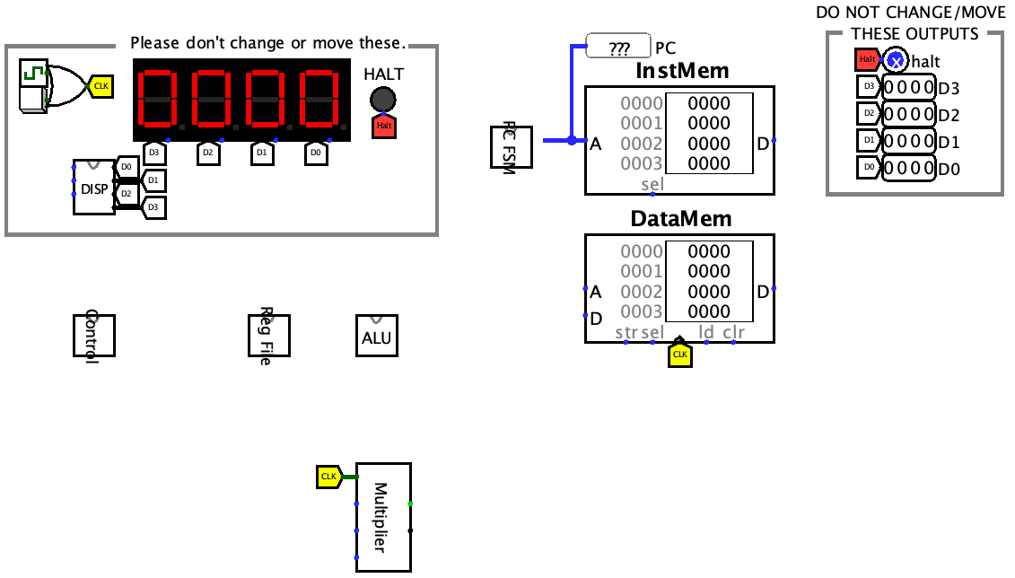
At the top is a box which contains, as it says, things that you should not change in any way or move around. Anything outside those boxes (InstMem, DataMem, PC FSM, Control, Reg File, ALU) can be moved around freely to your liking. (Things would get pretty cramped if you couldn’t move them around.)
- In the box:
- In the top-left is the clock, as always.
- Next to it is the display, same as it was on lab 8, but the register is in a component now.
- Next to that is the halt LED, which turns on when the programs end.
- And finally are the autograding outputs. Like it says, don’t change them or move them.
- Below the box is the Instruction Memory with the PC FSM and Control. Finally are the Register File, ALU, and Data Memory.
- All the components are empty right now, but they are placed in vaguely good spots for them. Again, you can move them around if you need room, but if you keep your wires short and use tunnels, you may not need to.
Eventually you will connect the rest of the CPU to these things through wires and tunnels.
The Instruction and Data memories
The Instruction Memory is a Memory > ROM component. ROM stands for read-only memory.
The ROM is super simple to use: put instruction address (i.e. the value of the PC register) into the left side, get instructions out the right side. I’ve also attached a probe to the A input so that you can see what the current PC is… once you build that. That will be very helpful in running the tests.
The Data Memory is a Memory > RAM component. The address and data to store go in the left side, the clock in the bottom (the triangle), and the data that is loaded comes out the right side.
The str input is the memory’s write enable signal. Most instructions don’t write to the memory, so you’ll have to hook something up to it. Ignore the sel, ld, and clr inputs! You will never need them!
Phase 1: making pieces
1. The ALU
The ALU is a combinational circuit. Remember, you’re allowed to use any of the built-in Logisim components - adders, subtractors, shifters, bit extenders etc.
The ALU is exactly the same as what you made in lab 7. If you finished that lab, you can reuse your work like so:
- In your project, double-click the ALU component on the left side to edit it.
- Open your lab 7 (yes you can have multiple things open in Logisim at the same time)
- Go into your lab 7’s ALU component, Ctrl/⌘A to select all, and Ctrl/⌘C to copy
- Use the Window menu to go back to your project
- Use Ctrl/⌘V to paste that stuff into your project’s ALU circuit
Do NOT use the Project > Load Library menu in Logisim. It’s neat, but makes it MUCH harder for us to grade, because now your project is split across multiple files. Please copy and paste as described above.
If you didn’t do the lab, there are more detailed instructions on how to build this in the lab 7 instructions.
The ALU component works like this:
- INPUTS:
- 8-bit
A - 8-bit
B - 3-bit
Operation
- 8-bit
- OUTPUTS:
- 8-bit
Result
- 8-bit
- BEHAVIOR:
- The
Resultoutput depends on whatOperationis chosen:- if
Operation = 000, then outputA + B - if
Operation = 001, then outputA - B - if
Operation = 010, then outputA & B - if
Operation = 011, then outputA | B - if
Operation = 100, then outputA ^ B(that’s XOR) - if
Operation = 101, then output~B(Ais ignored) - if
Operation = 110, then outputA << B[2:0] - if
Operation = 111, then outputA >>> B[2:0](logical, not arithmetic)
- if
- The
2. The register file
Again, this register file is exactly the same as what you made in lab 7. If you did that lab, you can do the same thing as you did with the ALU and copy it into your project’s Register File component. If you didn’t do that lab, well, you have to go do it now, because I’m not going to repeat the directions here.
I showed how to make the register file in class, and you presumably did it on the lab too. Details:
- 1 write port (3-bit
rdto select the register, 8-bitREG[rd]is the data input) - 2 read ports (3-bit
rsandrtto select the registers, 8-bitREG[rs]andREG[rt]are the data outputs) - one write enable input
- THIS is what you demultiplex, not
REG[rd]
- THIS is what you demultiplex, not
- one clock input
- 8 registers, 8 bits per register
- but register 0 is not a register - just a constant 0
3. The PC FSM
The PC is a register which holds the address of the current instruction. Since your instruction memory uses 8-bit addresses, what size should the PC register be? 😉
Remember from class that the PC can move ahead by 1 instruction, or jump to other places, or conditionally branch. That’s what this component is for. There is also an example PC FSM on the Materials page whose structure you can base yours on. But this time, don’t just copy and paste the circuitry; replicate it yourself. There are enough differences from the example that copying and pasting won’t really save you much time anyway.
It will have:
- INPUTS:
- 1-bit
Clock - 8-bit
Offset - 8-bit
Target - 1-bit
Jump - 1-bit
Branch - 1-bit
Halt
- 1-bit
- OUTPUTS:
- 8-bit
PC Out - 8-bit
PC+1 Out(for thejalinstruction’s return address)
- 8-bit
- BEHAVIOR:
- If
Haltis 1, the PC register is disabled. (This is backwards or inverted or logically negated from the normal behavior of the write enable input. HINT HINT.) - If
Jumpis 1,PCwill be set toTarget.- Else if
Branchis 1,PCwill be set toPC + Offset. - Else,
PCwill be set toPC + 1.
- Else if
PC+1 Outshould output whatever comes out of the adder.
- If
Like we said in class, how the branch conditions are checked are not really the responsibility of this component! That is explained later and done elsewhere.
Phase 2: the control and interconnect
Now What?
From here, things get a little weird. You have two more important things to make: the interconnect (connecting all the components together) and the control (tells all the components and the interconnect what to do for each instruction).
However, you can’t really make one without knowing something about the other. It’s technically possible to do all the interconnect before moving onto the control, but most people aren’t familiar enough with how the CPU works yet to be able to do that easily! So I will ease you into it for the first few instructions.
How the control and interconnect work together
Remember from the interconnect lecture that each instruction can make use of multiple components of the CPU. For example, a load instruction might:
- use the Register File to get the contents of one register
- use the ALU to add the contents of that register to the immediate, to calculate the address
- use the Data Memory (RAM) to load a value out of that address
- use the Register File again to put the loaded value into a register
The interconnect is all of the wires and multiplexers that connect the various CPU components together so that they can send the data to each other. However, none of these components can read instructions, and cannot do any work without being told what to do.
The control is what reads the instructions and tells all the CPU components - and the interconnect - what to do to implement each instruction. Remember: the control is the brain, and all the other parts of the CPU are the body.
“Where does the instruction’s work happen? In the control?”
No. The control doesn’t do any work itself. It isn’t adding numbers or loading values or anything. It just tells all the other parts of the CPU what to do, and when.
“Does the control need to take the registers/ALU output/loaded memory/etc. as inputs?”
No. Again, the control isn’t responsible for doing any work. It does not work on values. The only input to the control is the instruction coming out of the instruction memory (ROM).
“How does an instruction description like REG[rd] <- REG[rs] + REG[rt] get implemented?”
Well it’s good to keep in mind:
- what each part of your CPU is capable of doing, and
- how you tell it to do that (i.e. what inputs you have to give it).
It’s hard to explain an exact process for turning an instruction description into something the CPU can do, but that’s what the rest of this tutorial will try to do!
4.1 - Starting the control
If you did lab 8, this should be familiar to you now. If you didn’t… well, have fun!
Please go review your notes from the Control lecture, or get them from a classmate. There is also a decoding.circ example on the Materials page that shows many of the concepts in practice, but for a small subset of MIPS, not this project’s ISA. Lab 8 also had its own instruction set.
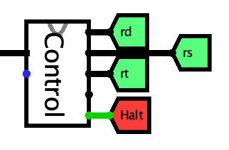
- Edit the Control component. Inside, its only input is the 22-bit instruction.
- (It does not have a clock input as it is a combinational circuit.)
- Split up the instruction input.
- There is only one format, documented on the ISA page.
- Use a splitter to split the instruction into its fields.
- The “fan out” is how many pieces to split the value into.
- Then you can adjust which outputs each bit goes to. The numbers on your splitter should match the numbers on the instruction format diagram.
- After splitting you should have these fields:
opcode(5 bits)rd,rs, andrt(all 3 bits)imm(8 bits)
- Decode the opcodes.
- Just like what we talked about in class,
decoding.circ, and lab 8, you’ll use a decoder. 5-bit opcode into a 5-bit decoder. - Create all the instruction signal tunnels connected to the outputs of the decoder. Look at the ISA to see which opcodes correspond to which instructions. It lists them all in numerical order (so, the same order as the decoder outputs).
- Name the tunnels coming out of the decoder like so:
hlt,put,li, etc. - Don’t waste space naming them
add rd, rs, rtor whatever! - And definitely DO NOT name them
00000,00001, etc. YOU ARE NOT A COMPUTER!!
- Name the tunnels coming out of the decoder like so:
- Just like what we talked about in class,
- Output the register indexes and immediate.
- Create 3 3-bit outputs named
rd,rs, andrt, and an 8-bitimmoutput. - Connect the
rd,rs,rt, andimmtunnels to them.
- Create 3 3-bit outputs named
4.2 The interconnect
The interconnect is not another component. It exists on the main circuit, connecting all the components of the CPU together.
So go to the main circuit, and you can start connecting them up. Here are the broad strokes:
- The clock signal is needed by several components:
- The RAM (already hooked up)
- The Display unit
- The Register File
- The PC FSM
- The PC FSM’s
PC Outoutput goes into the ROM’sAinput.- That’s the one with the probe on it.
- The ROM’s
Doutput goes into the Control’s instruction input. - The Control’s
rd,rs,rtoutputs go to the register file.- See, now the control is telling the register file which registers to access!
Some more tips:
- Use tunnels where they make sense. Tunnels let you name your wires and move the parts of your CPU around independently.
- Copy and paste tunnels when you need another of the same name. This avoids naming mistakes (e.g. naming one end
Instand the other endinst, which are different names).
4.3 The first instruction: hlt
Try ticking the clock right now by using the hand tool to click the clock button. The PC moves ahead. This is wrong.
See, the ROM is full of instructions that are all 0s, which is the hlt instruction. This instruction should halt the CPU, which means the PC should stop changing.
If you don’t believe me that this is a hlt instruction,
- Switch to the hand 👆 tool.
- On the main circuit, click on the control component so the magnifying glass 🔍 icon appears, and double-click it.
- You should see the “You are viewing the state of an embedded subcircuit” message at the top.
- You should see the
hlttunnel’s wire lit up.- If you’re ever unsure of what the current instruction is, you can just look at the opcode decoder’s output like this.
Alright, let’s make the halt instruction work. It has two effects:
- the PC FSM should halt, and
- the HALT LED on the main circuit should light up.
So do this:
- In the control:
- Add a 1-bit output to the control named “halt”.
- Duplicate the
hlttunnel from the decoder, and attach it to that output.
- On the main circuit:
- Conveniently, there is already a
Halttunnel next to the control. Connect it to the Control’shaltoutput. - Duplicate that tunnel and connect it to the PC FSM’s “halt” input.
- Conveniently, there is already a
- Now reset, and tick the clock. The PC should now stay at 0! You just implemented the
hltinstruction! or– Wait a second. Look at the instruction input to the control.
It got disconnected from the control!
So here’s a really really annoying feature of Logisim. Because we added more outputs to the control, it got taller, which made the instruction input move down, making it get disconnected from the instruction memory.
This drives me nuts. There are two ways to solve this:
- Every time you add more outputs to the control, you have to check on the main circuit to see if it came undone and reconnect it to the ROM. This is annoying.
- Go into your Control circuit, then Project > Edit Circuit Appearance. See the blue square on the left? Drag it up by 1 dot.
- Now go back to main and make sure it’s reconnected to the instruction tunnel.
- Once it is, you never have to do this again. Once you have edited the control’s appearance, the input will never move! And you can also edit its appearance to e.g. space out the outputs more so you can connect tunnels to it more easily.
- The only downside is, the rectangle won’t automatically get any bigger from now on, so you’ll have to edit the control’s appearance to make it taller.
Once you fix that, you did it! You implemented hlt!
At this point, the HALT LED at the top should be on (red) and the halt output should be 1, not x. In the past, people made their own Halt tunnel with a different name and broke the autograding halt output. Don’t be like them. Use the red Halt tunnel that I made for you.
4.4 The next instructions: li and put
The first real test program is the one that tests these instructions. Let’s actually do put first cause it’s simpler, but we won’t be able to test it until we implement li.
Implementing put
The put description says display <- REG[rs] : REG[rt]. This is telling us two things:
- How to connect the Display and the Register File together
- What should happen (the display should change)
So here’s what to do:
- The syntax
REG[rs] : REG[rt]means you need to concatenate the two 8-bit values together into a 16-bit value. This is a job for a splitter - they work both ways! They can concatenate values too. - Connect the
REG[rs]andREG[rt]outputs of the Register File to that splitter, and the splitter’s output to the “Data” input of the Display.- Use some dang tunnels named
REG[rs]andREG[rt]. - You’ll be copying and pasting those tunnels multiple times throughout the project!
- Use some dang tunnels named
- You need a new control signal.
- In the control:
- Make a 1-bit
Display WEoutput - Duplicate and connect the
puttunnel to it- This is because
putis the only instruction that writes to the display.
- This is because
- Make a 1-bit
- On the main circuit:
- make a
Display WEtunnel - use it to connect the control’s
Display WEoutput to the Display’sWEinput
- make a
- In the control:
That’s it! But here’s an important warning: hlt and put are extremely simple instructions, and you cannot just make an output for every instruction like this. These instructions are the exception, not the norm. The control circuitry for subsequent instructions is going to get more complex!
Implementing li
Finally, a non-trivial instruction. It says REG[rd] <- imm. What does that mean?
immis the immediate, one of the fields of the encoded instruction.- It’s one of the things coming out of the instruction splitter in your control.
REG[rd] <- immis again telling us two things:- that immediate needs to go into the register file’s
REG[rd]input; and - the register file’s write enable needs to be turned on for this instruction, so that the value will actually go into the register selected by
rd.
- that immediate needs to go into the register file’s
So here’s what you’ll do:
- On the main circuit, connect the control’s
immoutput to the register file’sREG[rd]input.- (This will change soon, but for now it’s all you need.)
- In the control, make a new control signal output,
Reg WE.- This is a 1-bit control signal, so we need to OR together all the instructions where we want it to be 1.
- Look at the ISA page and find all the instructions that have
REG[rd] <-in them.- Use your browser’s find (Ctrl+F/⌘F) tool to look for them.
- Duplicate the tunnels for those instructions from the decoder and make them face right, then OR them all together and connect the OR’s output to the
Reg WEoutput.
- On the main circuit, connect the control’s
Reg WEoutput to the Register File’sWEinput.
Testing the li and put instructions
Okay. Now that that’s dealt with, you can test it out by doing this:
- load the test program into the instruction ROM
- reset (Ctrl+R or ⌘R)
- then tick the clock manually (click the button on the “clock ticker” thing)
If all goes well, after a few cycles you should see 0053 on the display! One more cycle should show 7753, and finally it will show 0000 and it halts. (That test description also explains what could go wrong if you implemented things incorrectly.)
Hey, guess what, you now have a 42% on the project, and it (mostly) gets easier from here, honestly!
Intermission: testing registers
The next test tests that all the registers are working properly. That test should work correctly now, unless there is something wrong with your register file.
4.5 Implementing mov and the RegDataSrc mux
Then comes the test for the mov instruction, which you haven’t implemented yet. If you run the test now, it won’t work right. That’s because we hard-wired the immediate into the register file’s data input, which will work for li but nothing else. Instead we need to choose which value goes into the register file.
The RegDataSrc mux
On the main circuit, you need to set up a MUX on the register file’s input as so:
- Data bits: 8
- Select bits: 3
- Input 0 should be the ALU’s output (trust me, this will make things much simpler later)
- Input 1 should be
imm - Input 2 should be
REG[rs](formov, which we’re about to implement) - Select input should be a 3-bit tunnel named
RegDataSrc- Right now it’s not hooked up to anything but that will be the next thing you do.
Keep the order of the values on the inputs in mind.
Now in the control, you need to make the RegDataSrc control signal and output:
- Make a Plexers > Priority Encoder with 3 select bits
- Put a constant
1into its first (top) input on the left- This will make the “default” data source the ALU, and trust me, that saves a lot of work when you get to the ALU instructions. (Otherwise, you would have to OR together alllllllll the ALU instructions…)
- Copy the
litunnel, and connect it to input 1 of the encoder (the one right below the constant 1). - Copy the
movtunnel, and - Notice how the inputs to this encoder mirror the inputs to the
RegDataSrcmux.- Input 0 (the constant
1) makes the ALU output the “default” value to go into the reg file. - Input 1 (
li) says “if we are executingli, setRegDataSrcto 1”, which causes theimmto go into the reg file. - Input 2 (
mov) will causeREG[rs]to go into the register file.
- Input 0 (the constant
- The priority encoder’s output goes to a new 3-bit output named
RegDataSrc.
Finally on the main circuit, hook the RegDataSrc signal up to the mux. Don’t forget to do this!
Now the mov test should work. Notice that on each instruction when the register file’s WE is 1, RegDataSrc is set to a value that chooses the appropriate MUX input. Nice!
Now would be a good time to go back to make sure 01_li_put still works, too.
Okay!
It takes a good bit of work to get here, but you actually have pretty much all the skills you need to finish the project, as well as a good bit of the interconnect complete.
Proceed through the tests in the order they’re given, implementing the needed instructions as you go. Sometimes this will require you to change some circuitry you already built (like when we had to add the RegDataSrc MUX earlier). That’s okay. It’s okay to change your work.
Phase 3: the test programs
Each test assumes the previous tests work properly. If you can’t get one test working, don’t waste your time trying later ones, because they will probably break too. So, do them in order, and get the earlier tests done first. Ask for help if you are stuck. Correct implementation of a few instructions is worth more points than partial implementation of several instructions.
To run the tests:
- In your main circuit, right click your program ROM component and choose “Load Image”
- Open the
.romfile you want to run, which should be in the same folder if you followed the directions above. - Reset, save, and run it.
- The shorter programs are easier to test by single-stepping the clock, instead of having the clock tick automatically.
Finally, these rom files are just text files - you can open them in a text editor to see the source code on the right, as well as the PC for each instruction (in decimal), so you can figure out which instructions are tripping up your CPU.
0. The hlt instruction (00_halt.rom)
The simplest program ever: this should halt immediately. (It really is all 00000 instructions.)
The PC should not increment, and the HALT LED should turn on.
If the PC is changing (going 0, 1, 2, 3): either your control isn’t sending a halt signal to the PC FSM, or the PC FSM isn’t disabling the PC reg when the halt input is 1.
1. PLEASE GET THESE WORKING: li and put (01_li_put.rom)
This is a very short program, so it’s easiest to see if it’s working right by resetting, then ticking the clock manually (ctrl+T or ⌘T, or clicking the button you have ORed with the clock signal).
The output should change to 0053, then 7753, then 0000 again, and halt.
In more detail, this program does the following:
- PC = 0 uses
lito load the immediate0x53intor1- but remember that the effect of each instruction happens when you tick the clock; so this value will not actually be put into the register until you tick the clock and PC changes to 1.
- PC = 1 uses
lito load0x77intor2 - PC = 2 displays
0053on the numeric display by usingput r0, r1- again, you will not see the result of this
putinstruction until you tick the clock and PC becomes 3
- again, you will not see the result of this
- PC = 3 displays
7753on the numeric display by usingput r2, r1 - PC = 4 displays
0000on the numeric display by usingput r0, r0 - PC = 5 halts.
If the PC goes directly from 0 to 4, causing it to never display anything other than 0000, you’re not supposed to add 4 to the PC on each tick!!!!!!
If it shows something like 7777 you probably demultiplexed the data in the reg file instead of the write enable, which is wrong.
If it otherwise never displays anything, check:
- that register 1 holds
0x53when PC = 1- hand tool, double click on the register file component on the main circuit and have a look (you should be seeing a yellow background)
- if it doesn’t,
liis broken somehow. reset so that PC = 0 and make sure ALL of the following are true:- the register file’s write enable is turned on
- register 1 is being selected for writing (that is, the
rdsignal is001) - the immediate value
0x53is being selected to go into the register file
- if
liworks, something’s wrong with the way the display works, or how things are connected to it.
2. ALSO IMPORTANT: Checking the register file (02_allregs.rom)
This checks to see if all 8 registers can be written to and read from.
It will also “load” the immediate 0xFF into r0, which should do nothing.
This should appear to do nothing for several instructions, and then display the numbers 0011, 0022, 0033... up to 0077, then halt.
If you see FFFF as the first value, you implemented r0 wrong. It’s a constant 0, not a register.
If you only see 0000 for a while and then 0077, your write enable circuitry is messed up. Don’t use a demux for the data, use it for the write enable signal.
If there are missing numbers, or they come out in a weird order, step through and see what’s going into the registers after each li instruction. Be sure to double click on the component in the main circuit and not the name on the left side. Sometimes it’s easy to forget to connect one register’s write enable or data in the reg file component.
3. mov (03_mov.rom)
mov works like MIPS’s move instruction, but it’s a real instruction instead of a pseudoinstruction. It copies from one register to another.
This is a very short program. When it executes correctly, it should output 0092. The three instructions are as follows:
- It loads the immediate
0x92intor1 - It does
mov r2, r1(copies that value intor2) - It does
put r0, r2
If you only see 0000, then mov (which is at PC=1) isn’t working. Figure out why.
ALUOp and using priority encoders the right way
You’re about to make the control logic for the ALUOp control signal, which is 3 bits. That means you need a priority encoder with 3 Select Bits.
People often get confused about how to use priority encoders the right way, so start with the thing on the right. You always need to put a constant 1 into the 0 input to avoid blue wires.
But that constant 1 automatically handles ALUOp 0, which if you did your ALU like was specified in lab 7, is the addition operation. That means you do not need to do anything to make the instructions that add (e.g. add, adi, ld, st) work properly. They’re done.
Input 1 of the priority encoder is for ALUOp 1, which again if you followed the lab, is subtraction. So you will OR together all the instructions that need to perform subtraction. Then input 2 is for ALUOp 2, etc.
Control and Interconnect Intermission 1: the ALU
You are about to implement the ALU instructions. So go look at them on the ISA reference. You already built the ALU to perform all these operations. So, what are the inputs to the ALU going to be? Go look at the dummy_cpu.circ example. It’s gonna be veeeery similar. Like…………………. the same. It’s the same okay
That ALUBSrc MUX needs to be controlled. It’s just a 1-bit control signal, so you know what to do there.
As for RegDataSrc, as long as you followed my advice and used the ALU output as input 0 to that mux, then you’re already done. If you didn’t, well, have fun ORing together all the ALU instructions in the control to pick the ALU’s output for RegDataSrc :)
4. Basic ALU: add, sub, and, or, xor, not, shl, shr (04_alu_basic.rom)
You uh, you did the stuff in the above two intermissions right? “Intermission” does not mean “optional.” :)
This program is a bit longer, and will display 8 different numbers. They will appear in this order (the things in the parentheses are what produced that value):
0096(add: 30 + 120)005A(sub: 120 - 30)0018(and: 30 & 120)007E(or: 30 | 120)0066(xor: 30 ^ 120)0087(not: ~120)00F0(shl: 120 << 1)003C(shr: 120 >>> 1)
If it just displays 0000 until it halts, did you actually do the interconnect to the ALU like I told you in the previous section? If nothing is going into the ALU, it’s just gonna output 0s. The other possibility is that your RegWE signal is wrong and not being turned on for them.
If all you see is 0000 and 0078, look for blue wires on your main circuit. If you don’t actually tell a mux what to select, it will output blue. Fix that.
If several or all the answers are wrong, maybe there’s something up with the way you come up with the ALU Operation control signal.
If only one is wrong, maybe that part of your ALU needs a look. Remember, you can see what instruction is at each PC by looking inside the control unit and seeing what the decoder says it is.
5. Immediate ALU: adi, sbi, ani, ori, xri, sli, sri (05_alu_imm.rom)
Again, this will display several numbers:
0050(adi: 50 + 30the output is hex, so decimal 80 is0x50)0014(adi: 50 + (-30))0050(sbi: 50 - (-30))- If this is
004finstead, your adder and subtractor are touching in your ALU. Separate them so thec outof the adder is not connected to the subtractor’sb in.
- If this is
0014(sbi: 50 - 30)0012(ani: 50 & 30)003E(ori: 50 | 30)002C(xri: 50 ^ 30)00C8(sli: 50 << 4)000C(sri: 50 >> 4)
If they all fail, maybe your data going into the ALU’s “B” input is wrong. It should be choosing the immediate value, not the register value.
Control and Interconnect Intermission 3: the data memory and rt
The next test is the load and store instructions for accessing data memory. Once again, go look at the ISA for these two instructions, and revisit the dummy_cpu.circ example. It’s gonna be the same as that, again. The ALU produces the address for the memory, and REG[rt] goes into the D input on the left side.
RegDataSrc definitely needs to be updated, since the D output on the right side of the data memory needs to go into the register file. Remember that not every instruction writes to the register file, so not every instruction must choose something for RegDataSrc. (To put it another way, it’s okay if RegDataSrc is 0 for st, because st doesn’t put anything in the register file, so the value going through the MUX will just be ignored.)
You may have to update your ALUBSrc control to include ld and st, since these also perform “register + immediate.”
You shouldn’t have to update ALUOp since, again, the constant 1 handles addition for you.
Finally, the data memory needs a write enable signal (MemWE). That goes into the str (“store”) input of the data memory. Hey - DOES ld WRITE INTO MEMORY?
Do not use the RAM’s ld input for the ld instruction. I know it’s tempting. Just don’t. Never connect anything to the RAM’s ld, sel, or clr. Otherwise: blue wires.
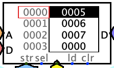
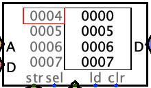
6. RAM: ld and st (06_ld_st.rom)
Let’s see if the RAM works. The display should stay 0 for a while, then display 0005, 0006, 0007, then halt.
- The first 3 instructions (PC = 0, 1, 2) load immediates into
r1, r2, r3; - the next 3 (PC = 3, 4, 5) store into memory locations
0, 1, 2; - the next 3 (PC = 6, 7, 8) load those values back into
r4, r5, r6; - and the last 3 (PC = 9, 10, 11) display
r4, r5, r6(which should show0005,0006,0007).
At the end of the program, use the hand tool to click the address column on the RAM (the grey numbers on the left) and type 0000. It should look like this:
If you only see 0001 and 0002 at the end, there are a few possibilities:
- You didn’t handle
rtthe way I said to in the previous section RegDataSrcisn’t correctly picking the RAM output for theldinstruction
If nothing is displayed (just 0000 the whole time),: at the end of the program click the address column and type 0004. If you see this (0001 and 0002 in RAM at addresses 0006 and 0007):
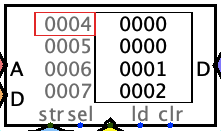
Then you swapped the address and data inputs to the Data Memory (RAM). The ALU output is the address.
If instead you see this in RAM:
Then your ALU is doing REG[rs] + REG[rt] when it should be doing REG[rs] + imm. make sure the second input to the ALU is the immediate for both ld and st, just like all the immediate ALU instructions.
If all the RAM values are 0000 instead, you probably aren’t turning on the RAM’s write enable (the str input) for st.
If your RAM looks correct, but it displayed all 0000, look in your register file after the program halts. r4, r5, and r6 should hold 5, 6, and 7. If they don’t, your ld is wrong. Chances are, you forgot to turn on the register file’s write enable for ld.
7. More tests of ld and st (07_ld_st_2.rom)
This one tests the address calculation of these instructions. Basically it does:
- PC = 0
r1 = 8 - PC = 1
r2 = 9 - PC = 2
r3 = 2 - PC = 3
MEM[r3 + 1] = r1address 0x03 should now hold 8 - PC = 4
MEM[r3 + -1] = r2address 0x01 should now hold 9 - PC = 5
r3 = 3 - PC = 6
r4 = MEM[r3 + 0]r4should now hold 8 - PC = 7
r3 = 1 - PC = 8
r5 = MEM[r3 + 0]r5should now hold 9 - PC = 9 displays
r4should show0008 - PC = 10 displays
r5should show0009
If the addresses are REALLY off and it’s accessing some address other than 0x0001 at PC = 4, uhhhhhhhhhhhhhhhhhhhhhhh idk lol
Control and Interconnect Intermission 4: jumps and the return address
Look at the jump instructions in the ISA. There are 3, but they are kind of all related to each other j and jal both use imm as the target. j and jr simply jump, but jal also links (puts the return address in rd).
Your control needs to output a couple things for these to work:
- the
Jumpcontrol signal for the PC FSM - this should be 1 for any kind of jump - some signal saying which value to use for the jump target (hint: there are only two options…)
Then for the interconnect, you need to connect that Jump signal to the PC FSM, and then make a circuit to choose what the PC FSM’s Target input should be.
You also need to connect the PC FSM’s PC+offs output to the RegDataSrc mux, which means you need to update its control to handle jal.
8. j (infinite loop) (08_j.rom)
This should loop infinitely, displaying an increasing count on the display (0001, 0002, 0003, 0004 etc.). Try doing Simulation > Enable Ticks and turn up the tick frequency… wheeee!!!
The PC (that is, the probe on the address going into the instruction memory!) should go 0, 1, 2, 3, 1, 2, 3, 1, 2, 3...
The j is at PC = 3. At PC = 3, your PC FSM inputs should be:
Jump = 1(that is, “yes, we are jumping”)Jump Target = 0000 0000 0000 0001(the immediate)
If it halts, then your PC FSM probably isn’t being told that j is a jump.
If it loops, but just shows 0001 forever, and the PC goes back to 0 after 3, then the PC FSM’s jump target is probably wrong. It’s supposed to be the immediate.
9. jr (09_jr.rom)
The jr instruction works just like j, except instead of using the immediate as the jump target, it uses REG[rs] as the jump target.
This is a very short program. The jr is located at PC = 1, and it will try to jump to address 5.
On success, it will output 0001 and halt. (The PC will go “0, 1, 5, 6, 7” in that case.)
If it outputs FFFF instead, that means your jr didn’t jump. Your PC FSM’s “jump” control signal should be 1 if you are executing any of the jump instructions (j, jr, jal, or jlr).
If it loops infinitely with the PC going 0, 1, 0, 1, 0, 1…, that means your jr is using the wrong target. It’s probably using the immedate, when it should be using the value of REG[rs]. j and jal use the immediate as the target; jr uses REG[rs] as the target. CHOOSE.
10. jal (10_jal.rom)
jal works a little different from MIPS’s jal since it lets you specify which register to put the return address in, but this test program will use r7 as the return address register.
This is another very short program. The jal is located at PC = 1, and it will try to jump to address 5, putting the return address (2) into register 7.
On success, it will output 0002 and halt. (The PC will go “0, 1, 5, 6” in that case.)
- If it outputs
FFFF, that meansjaldidn’t jump.- Your PC FSM’s “jump” control signal should be 1 if you are executing any of the jump instructions (
j,jr,jal, orjlr).
- Your PC FSM’s “jump” control signal should be 1 if you are executing any of the jump instructions (
- If the PC goes “0, 1, 5, 6” but it outputs
FFFEinstead, that means yourjalis jumping to the target correctly, it could be either:- you didn’t do the
rddecoding right as explained in the previous control and interconnect intermission; or jalnot turning on the register file’s write enable. Time to update the control forRegWE!
- you didn’t do the
- If the PC goes “0, 1, 5, 6” but it outputs
0000, it could be that:- your
RegDataSrccontrol isn’t choosing thePC+offsoutput of the PC FSM. - that value just isn’t connected up on the main circuit.
- your
- If it loops infinitely with the PC going 0, 1, 0, 1, 0, 1…, that means your
jalis using the wrong target. It’s probably usingREG[rs], when it should be using the immediate.jandjaluse the immediate as the target;jrusesREG[rs]as the target. CHOOSE.
11. jal and jr together (11_jal_jr.rom)
This program should output 0001, 0000, 0002, 0000, 0003 and then halt. It does the equivalent of:
f1();
put(1);
f1();
put(2);
f2();
put(3);
halt;

void f2() { f1() }
void f1() { put(0); }
The PC should go in this sequence (this is in decimal):
0, 1, 2, 3, 16, 17, 4, 5, 16, 17, 6, 7, 10, 11, 12, 16, 17, 13, 14, 15, 8, 9 (halt)
If it goes like 0, 1, 2, 3, 4, 5, 6, 7, 8, 9 and displays 0001, 0002, 0003, then jal isn’t actually jumping anywhere. The first jal is at PC = 3. Investigate!
If it goes like 0, 1, 2, 3, 16, 17, 0, 1, 2, 3, 16, 17, ... in an infinite loop, there are a few possibilities:
- extremely common mistake: you are not write-enabling the register file for
jal, so the return address is never saved into register 7. - if it is going into that register, then either:
jris not using the correct value for the jump target input to the PC FSM;- or the return address isn’t getting pushed or popped to the stack correctly. (did you break the
ld/stinstructions somehow? go back to the tests for those.)
If it goes like 0, 1, 2, 3, 16, 17, 3, 16, 17, 3, 16, 17, ... in an infinite loop, you forgot to use PC + 1 as the return address (i.e. the value coming from the PC into the register file).
If it does something else… I dunno!! Go back to the earlier jr and jal tests!
Control and Interconnect Intermission 5: Branch instructions
The next group of instructions is the branch instructions (blt, bge, beq, bne).
- you need a new control signal that says “the current instruction is a branch”
- you need another new control signal that says which of the four conditions is being tested (
<,>=,==, or!=).- Hmm… four possibilities… how many bits is this control signal going to be?
- write down which comparison condition value means which operation so you don’t have to keep looking back at this!
- the
ALUOpcontrol needs to be updated to do a COMPARISON for any of the branch instructions.- I say COMPARISON, you say…………what????!!!!!!!!!!
Finally you need to actually check the branch condition on the main circuit.
- You have compare the ALU’s output to 0 (make sure that comparator is set to 2’s complement!!).
- You have 4 different conditions to check - all of them can be produced with just one comparator.
- Then you need to choooooooooose which of the 4 conditions you want to look at.
- Remember, do everything, pick only the thing you care about.
- Finally, you need to AND that with the control signal that says “this is a branch,” and that is your PC FSM’s
Branchinput.- We only want to branch if the current instruction is a branch AND its condition is satisfied.
Your PC FSM handles changing the PC already. If its Branch input is 1, it will add the offset to the PC, otherwise it adds 1 to it. What you have to implement is the logic that comes up with the PC FSM’s Branch input, and connect the immediate to the branch offset input. (Again, you handled the immediates in the control already.)
Here are some common questions and answers:
- My branches are ALWAYS (or NEVER) branching!
- The branch should happen only when:
- The current instruction is a branch, AND (as in, use an AND gate lol) the branch’s condition is satisfied.
- It’s easy to only check for one of these and forget to check the other.
- The branch should happen only when:
- Logisim gives me an “Oscillation apparent” error and stops my simulation.
- You are doing Weird Shit ™️ with the
Ainput to the instruction memory. Don’t. The current value of the PC is what goes into the instruction memory’sAinput. Yes, even for branches. You never have to change that part. Branch instructions change what the next PC is by turning on the PC FSM’sBranchinput.
- You are doing Weird Shit ™️ with the
12-15. Conditional branching: blt, bge, beq, bne (12_blt.rom through 15_bne.rom)
These are all for loops which should output a sequence of numbers and then halt. Here are the tests and the numbers they should output:
12_blt.rom:0010,0011,0012,0013,0014,0015, then halt13_bge.rom:0015,0014,0013,0012,0011,0010, then halt14_beq.rom:0001,0002,0003,0004,0005, then halt15_bne.rom:0005,0004,0003,0002,0001, then halt
If they’re behaving strangely and the PC is going all over the place, make sure you are calculating the branch target correctly. It’s the current PC value (not PC + 1!) plus the immediate.
If the loops end one number too early or too late, or they never end, your branch condition checking logic is the likely culprit.
16. Signed comparisons (16_sign_cmp.rom)
This checks that your comparison instructions are performing signed comparisons instead of unsigned ones.
Done correctly, it will output 0001 (if bge is working right) and then 0002 (if blt is working right).
If it displays BADD, it means your branch condition comparator is set to do unsigned comparison. Change it to 2’s complement.
17. Finding primes (17_primes.rom)
Finally, a real program. This is a prime-number-finder. It runs forever, and will output the sequence of prime numbers: 0002, 0003, 0005, 0007, 000b, 000d, 0011, 0013, 0017… well, it’s in hex, so they’ll look a little funny, but hey.
This is a very slow program, so turn on ticks (Simulate > Ticks Enabled) and set the Simulate > Tick Frequency to a large value. The first few numbers will be found very quickly. But the bigger the numbers get, the longer it will take to find them. Even at 4KHz, it will take several seconds for each.
If you’re curious, the algorithm this uses is incredibly stupid. It does something like this (but written in a very weird way):
- It prints 2, since that’s the first prime
- Then, for each candidate prime starting at 3 (so every odd number lol):
- It tries dividing that candidate by every odd number less than it, using division by repeated subtraction, you know, the exponential time algorithm lmao
- If any of them divide evenly, it’s not prime and we skip to the next odd candidate
- If none of them divide evenly, it’s prime! So print it
18. Recursive function (18_sum.rom)
A real program with a recursive function and a call stack! If everything else worked until now, this should work. This program uses most of the kinds of instructions your CPU can run - output, loading immediates, arithmetic, loads, stores, calls, returns, and branches - so it’s a good test of everything up to this point.
It will push a bunch of things “on the stack” (starting at address 0 in memory), then pop them, and then it should output 0037 and halt.
This program will take a while to run, so set the tick frequency higher and let it run on its own. When run at maximum speed (4KHz), this should finish within a second or two. If it’s going for several seconds at max speed, maybe it’s going into an infinite loop…
It does something like:
put(sum(10));
halt;

int sum(int x) {
    if(x == 1)
        return 1;
    else
        return x + sum(x - 1);
}
sum is a recursive function that calculates the sum of integers from 1 to n. So, sum(10) should give 55, or 0x37 in hex.
It uses r6 as the stack pointer, and initializes it to 0 at the beginning of the program. The stack grows upwards in this program, so each time it pushes something, it will appear at successive memory addresses (0, 1, 2, 3…). This makes it easier to see those values.
If you’re having problems with it, you can right-click the RAM component, click “Edit Contents”, and view the contents of the stack that way. It should look something like (starting at address 0 and moving right) 03, 0a, 0d, 09, 0d, 08, 0d, 07, ....
And that’s it! That’s all the tests!
When you’re done with the last test, re-run all the tests, to make sure you didn’t break anything along the way!
Submission
Be sure to review the grading rubric before submitting.
Gradescope will test your project rigorously by running programs on it.
If you need to resubmit, that’s fine. The last thing you submit is what we grade.
It is okay to submit on/before the normal due date, and then resubmit on the late due date. You will get the late penalty, but if you turn in a 60 on time and a 100 late, that 100 becomes a 90, and it’s a net win anyway!
Reminder that if you submit a file that cannot be opened (e.g. you used Logisim’s “Project > Load Library” feature) and we have to ask you for a fixed version, that is a 20 point penalty. That penalty is in addition to the late penalty.