In this lab, you’ll be building the control unit for a small… thing. It’s somewhere between an FSM and a real CPU. It has most of the same parts as a real CPU, and it reads and executes instructions like a real CPU does, but it can’t make decision, so… whatever. That’s not important. What’s important is that this will give you good practice for making the control unit for your project.
0. Starting point
Right-click and download these 4 files, and put them in the same folder on your computer. Then rename abc123_lab.circ with your username and open it in Logisim.
You cannot double-click abc123_lab8.circ to open it in Logisim. You have to run Logisim and use File > Open to open it.
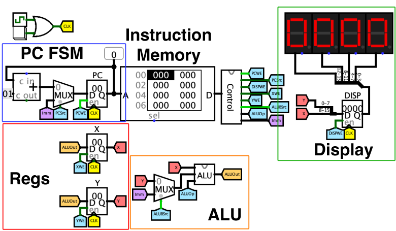
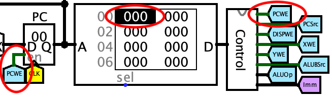
When you open it you will see a circuit already there. The diagram below explains what each part is for. The PC’s value is used as the address into the instruction memory, which outputs the current instruction; that goes into the control, which produces all the control signals and the imm tunnel as well.
Now look inside the Control unit by double-clicking its name on the left. You’ll see an input and some outputs, and that’s about it.
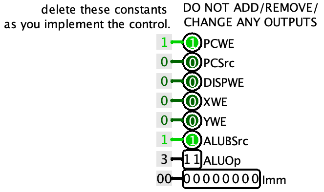
The outputs are currently hard-wired to output some constant values. As you work, you will be deleting those constants and replacing them with circuitry that implements each of the control signals.
Your Task
Your task is to implement the control unit for this circuit so that the test programs operate as expected. You will do all your work inside the Control subcircuit, and like the messages in there say, do not add, remove, or change any of the inputs or outputs. This is for autograding purposes (and like, you don’t need any more anyway).
Remember that the job of the control unit is to:
- take an encoded instruction as input;
- break it up into pieces, including the opcode;
- use the opcode to determine values for each control signal output; and
- output those control signals to the rest of the CPU.
The ISA
The instruction set architecture for this… thing is pretty simple.
Registers
- There are two 8-bit registers,
XandY, which are used to do computation. - There is one 16-bit register,
DISP, which is used to display numbers on the digit displays. - There is one 8-bit program counter,
PC.
Memory
There is only a 256-entry word-addressed read-only instruction memory. It is addressed by the PC register, and each entry contains one instruction.
Instruction format
There is only one instruction format, and all instructions are 12 bits:

Because instructions are 12 bits, they can be written as 3-digit hex numbers, where the first hex digit is the opcode and the other two are either an immediate value, or 00, depending on the instruction.
Instruction set
In the instruction descriptions below, the <- means “copy the value on the right into the register on the left.” It’s like an assignment operator in a programming language, but, if there are multiple <- operators in one instruction (like clr), they all happen simultaneously in one clock cycle.
This is all the instructions it supports, including their encoding (shown in hex), their mnemonic (their name), and a description of what they do. On the right are the control signal values that your control unit will output for each instruction. You don’t have to understand everything here yet, it’s just here so you can refer back to it.
| Encoding (hex) | Mnemonic | Description | ALUOp | ALUBSrc | XWE | YWE | DISPWE | PCSrc | PCWE |
|---|---|---|---|---|---|---|---|---|---|
0x000 |
hlt |
disable PC | xx |
x |
x |
x |
x |
x |
0 |
0x1nn |
lix imm |
x <- imm |
11 |
1 |
1 |
0 |
0 |
0 |
1 |
0x2nn |
liy imm |
y <- imm |
11 |
1 |
0 |
1 |
0 |
0 |
1 |
0x300 |
clr |
x <- 0y <- 0 |
11 |
1 |
1 |
1 |
0 |
0 |
1 |
0x400 |
put |
disp <- x:y |
xx |
x |
0 |
0 |
1 |
0 |
1 |
0x500 |
mxy |
x <- y |
11 |
0 |
1 |
0 |
0 |
0 |
1 |
0x600 |
myx |
y <- x |
10 |
x |
0 |
1 |
0 |
0 |
1 |
0x700 |
adxy |
x <- x + y |
00 |
0 |
1 |
0 |
0 |
0 |
1 |
0x8nn |
adxi imm |
x <- x + imm |
00 |
1 |
1 |
0 |
0 |
0 |
1 |
0x900 |
adyx |
y <- y + x |
00 |
x |
0 |
1 |
0 |
0 |
1 |
0xA00 |
anxy |
x <- x & y |
01 |
0 |
1 |
0 |
0 |
0 |
1 |
0xBnn |
anxi imm |
x <- x & imm |
01 |
1 |
1 |
0 |
0 |
0 |
1 |
0xC00 |
anyx |
y <- y & x |
01 |
x |
0 |
1 |
0 |
0 |
1 |
0xDnn |
jmp imm |
pc <- imm |
xx |
x |
0 |
0 |
0 |
1 |
1 |
1. The hlt instruction
The hlt instruction’s description says “disable PC.” On the main circuit, you can see that the PC’s write enable input has a tunnel connected to it, PCWE. That tunnel comes from the control unit.
If you tick the clock, you will see the PC increment with each cycle. This is incorrect, because the instruction memory is full of 000 instructions, which should be disabling the PC.
The behavior of the hlt instruction is very simple - just turn off the control’s PCWE output! - but we have to do a few things before we can get there.
1.1 Splitting up the instruction
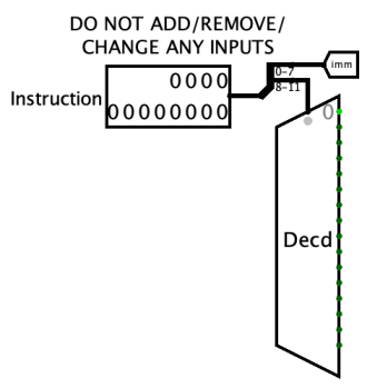
Inside the control, the very first thing you need to do is split up the instruction into its fields, according to the format(s) given in the ISA. This ISA is super simple: only one instruction format where bits 0-7 are the immediate and bits 8-11 are the opcode.

To split up the instruction, you need a splitter (Wiring > Splitter). Set its Bit Width In to 12 and its Fan Out to 2. You should have something like the image to the right.

The Fan Out property of splitters specifies how many pieces the input value should be split into. By setting it to 2, that means we’re splitting the 12-bit value into 2 pieces, one for the opcode and one for the immediate. But you can see the bits written on the splitter outputs, and they’re not right. Logisim splits up the bits evenly by default. What you want is for the splitter to look like this. Change the Bit 6 and Bit 7 properties of the splitter to make that happen.
Now you can connect the instruction input to the angled end of the splitter. You are now splitting up the instruction.
While you’re at it, delete that 00 constant currently attached to the Imm output of the control, and then connect the 0-7 output of the splitter to that output with a tunnel. There’s nothing more that we need to do with the immediate.

Bits 8-11, however..
1.2 Decoding the opcode
Bits 8-11 of the instruction are the opcode, the unique number that identifies each instruction. We will decode it with a decoder, like we talked about in class.
- Make a Plexers > Decoder with its Select Bits set to 4.
- (because the opcode is 4 bits.)
- Change its Select Location to Top/Right too, for convenience.
- Put it below the instruction splitter, and connect the
8-11output of that splitter to its select input.
You should have the circuit on the right now. Try using the hand tool to poke the upper 4 bits of the instruction input; you should see different outputs of the decoder lighting up.
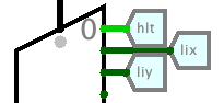
Now you need to make 14 tunnels, one for each instruction, connected to outputs 0 through 13 of the decoder. Go look back at the ISA table to see which number corresponds to which instruction. Name each tunnel the instruction’s name, but you don’t have to e.g. write lix imm, just lix is enough, because every instruction’s name is unique. Just don’t number your tunnels e.g. 0000, 0001, 0010. You’re not a computer.
Here are the first few tunnels. If you stagger them like this, you can keep this decoding very compact. Now you make the rest! The last two outputs of the decoder won’t be used, and that’s okay.
1.3 Implementing hlt
| Mnemonic | … | PCWE |
|---|---|---|
hlt |
… | 0 |
lix imm |
… | 1 |
liy imm |
… | 1 |
clr |
… | 1 |
put |
… | 1 |
mxy |
… | 1 |
myx |
… | 1 |
adxy |
… | 1 |
adxi imm |
… | 1 |
adyx |
… | 1 |
anxy |
… | 1 |
anxi imm |
… | 1 |
anyx |
… | 1 |
jmp imm |
… | 1 |
Okay, now we can actually implement the hlt instruction. To the right I’ve reproduced just a couple columns of the instruction set given above. PCWE stands for Program Counter Write Enable and it does exactly what it says. You’ll notice that hlt is the only instruction for which PCWE is 0.
Each of the tunnels coming out of the opcode decoder will carry a 1 if the current instruction is that instruction, and a 0 if not. So the hlt tunnel will be 1 when executing a hlt instruction. We want PCWE to be 0 when executing a hlt, and 1 otherwise. In other words:
if hlt is… |
then PCWE should output… |
|---|---|
| 0 | 1 |
| 1 | 0 |
:)
:)
gee I wonder what gate this is!!!!!!!!!!!!!!!!!!!
If you implement that correctly, you should now be able to go back to the main circuit, and see this:
That is, the control is now outputting a 0 for PCWE when the current instruction is 000. Now, when you tick the clock, the PC doesn’t change! WOOOOOOOW!
…
Okay yeah it’s kind of anticlimatic, huh. Well fine! The next instructions are more interesting!
2. lix, liy, clr, and put
First let’s look at the next few instructions in the table:
| Encoding (hex) | Mnemonic | Description | ALUOp | ALUBSrc | XWE | YWE | DISPWE | PCSrc | PCWE |
|---|---|---|---|---|---|---|---|---|---|
0x1nn |
lix imm |
x <- imm |
11 |
1 |
1 |
0 |
0 |
0 |
1 |
0x2nn |
liy imm |
y <- imm |
11 |
1 |
0 |
1 |
0 |
0 |
1 |
0x300 |
clr |
x <- 0y <- 0 |
11 |
1 |
1 |
1 |
0 |
0 |
1 |
0x400 |
put |
disp <- x:y |
xx |
x |
0 |
0 |
1 |
0 |
1 |
lix loads an immediate into X, and liy does the same for Y. clr clears both registers to 0. put puts a value on the display, but we’ll talk about that a little later.
Notice the ALUOp output for lix, liy, and clr must be binary 11, and the ALUBSrc output must be 1. I’ve hard-wired both of those outputs to those values, so we won’t have to worry about them yet. But what do the values of ALUOp mean? For that, you have to look inside the ALU.
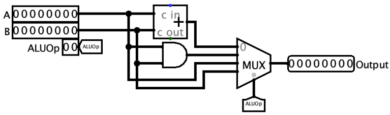
ALUOp will cause the ALU to perform the following operations:
ALUOp |
Output |
|---|---|
00 |
A + B |
01 |
A & B |
10 |
A |
11 |
B |
From this we can see that 11 causes the ALU to output its second (B) input. (It might seem odd to have the ALU just output one of its inputs as an “operation” but this is actually kind of a common thing to have in real ALUs; it makes instructions like “copy from one register to another” much easier.)
Then, if you look at the main circuit, you can see that the second ALU input is the output of a MUX, which is controlled by the ALUBSrc control signal. ALUBSrc stands for “ALU B input Source”, and controls the source of the data that goes into the ALU’s B input. When it’s 1, immediate is sent to the B input of the ALU. This is very much like what we saw in class.
So this is how the lix instruction works:
ALUBSrc = 1makes the ALU B input the immediate;ALUOp = 11causes the ALU to output the B input, so it outputs the immediate; andXWE = 1enables writing to theXregister, whose input is the ALU output.
Implementing XWE and YWE
XWE and YWE are the write enables for the X and Y registers, respectively. Since they are only 1 bit each, their control circuits will just be OR gates.
- Look in the full ISA table, and find all the instructions where
XWEis 1.- You can ignore
hltwhere it’sx, we’ll talk about that later. - You should find 7 instructions where
XWEis 1.
- You can ignore
- Select all 7 of those tunnels from the opcode decoder (shift+clicking will add to the current selection), then copy and paste them.
- Make an OR gate, set it to 7 inputs, and connect those copied tunnels to it.
- The output of that OR gate is
XWE; connect it to the control signal output with a tunnel. - Repeat the above steps for
YWE; only 5 instructions write toY.
The first test program
First, open lab8_test1.rom in your code editor of choice. Just… drag it in there. It’s fine. File extensions are meaningless. You’ll see:
v2.0 raw
1f0 # (PC = 0) lix 0xF0
20d # (PC = 1) liy 0x0D
400 # (PC = 2) put
300 # (PC = 3) clr
400 # (PC = 4) put
000 # (PC = 5) hlt
The 3-digit hex values on the left are the encoded instructions. The # and everything after them are comments that I put in there to show what the instructions actually are, and what address they are at (the PC = 0 etc.).
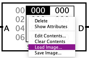
To run this program in your computer-thing:
- Go to the main circuit.
- Right-click on the instruction memory in the middle of the circuit.
- Click “Load Image…”
- Choose
lab8_test.rom.
The ROM’s contents will change to 1f0 20d....
Now to run the program:
- Reset (Ctrl+R/⌘R).
- Tick the clock with the hand tool (pressing the button is the easiest way to do that).
Here’s what you’ll see:
- When
PCis 1,Xwill now containf0. - When
PCis 2,Ywill now contain0d. - When
PCis 3… nothing seems to happen. - When
PCis 4,XandYwill now contain00. - When
PCis 5, the program stops running (PCWEbecomes 0), and you can’t go past 5.
“Why are all my registers changing one cycle later than they should?”
Compare what just happened to the instruction comments in lab8_test.rom. Does something seem… off? For example, lix 0xF0 is at address 0. But we don’t see the value of X change until PC increments to 1. In fact, all of the instruction effects seem to happen “one cycle later” than where they are written Did we do something wrong?
No! This is totally normal. Remember that all the registers in our circuit are triggered on the rising edge of the clock, including the PC register. This means that when we tick the clock, both X and PC change at the same time.
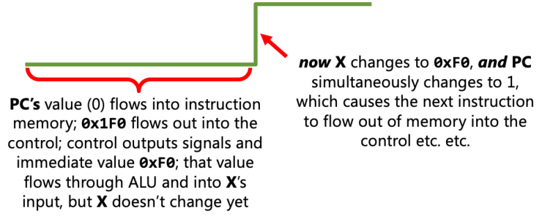
Very important thing to remember: each instruction is finished by the rising edge of the clock, and the next instruction begins immediately after. This makes it look like the results of instructions are “one clock cycle late” but they’re not. It’s all working as expected.
Implementing DISPWE, and “don’t care” outputs
There are two put instructions in the lab8_test1 program that didn’t work yet, because you didn’t implement the DISPWE control signal. Well, you can implement that now. It’s extremely simple. Simpler than PCWE. Go ahead. You can probably figure out how to do it :)
But there are a couple things that look weird about its row in the instruction set. One is the Xs in the ALUOp and ALUBSrc columns:
| Encoding (hex) | Mnemonic | Description | ALUOp | ALUBSrc | XWE | YWE | DISPWE | PCSrc | PCWE |
|---|---|---|---|---|---|---|---|---|---|
0x400 |
put |
disp <- x:y |
xx |
x |
0 |
0 |
1 |
0 |
1 |
“Don’t care” outputs are a little different than “don’t care” inputs. “Don’t care” outputs mean “you can output either a 0 or a 1, and it will have no effect either way.” For put, because both XWE and YWE are 0, then it literally doesn’t matter what the ALU is doing, because its results will be thrown away. Hence, don’t cares.
The other is the description: disp <- x:y. DISP is a 16-bit register, and X and Y are 8-bit registers. The syntax x:y means something like “the bits of X concatenated with the bits of Y.” That’s what that splitter on the input of DISP is doing: combining those two 8-bit values into a 16-bit one.
lab8_test1 should now work properly!
Here’s what it should do:
- set
Xtof0 - set
Yto0d - display
f00don the display in the top-right - set
XandYto00 - display
0000on the display in the top-right - halt.
Cool!
3. Implementing ALUBSrc and ALUOp.
Let’s speed up a bit. ALUBSrc is a 1-bit control signal. You know what to do with those now: OR together all the instructions where it needs to be a 1.
Then there’s ALUOp. This one is trickier, because it’s a 2-bit signal. This is where a priority encoder comes in handy.
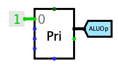
- Make a Plexers > Priority Encoder.
- Set it to 2 Select Bits. This will give it 4 inputs.
- Make a 1-bit Wiring > Constant, set to the value 1, and connect it to the top input on the left side of the priority encoder.
- The black output on the right side should go to the
ALUOpoutput of the control.
You should now have the thing on the right. Notice also that it is outputting 00 for ALUOp now - that’s because it sees a 1 on input 0, so it outputs the number of the input where it sees a 1. Which is 0. Aaa.
Now do the other inputs:
- Input 1 is right below the constant 1, and into it, you should put the output of an OR gate of all the instructions that need
ALUOpto be01. - Below that is input 2… you got it, all the instructions that need
ALUOpto be10(2). There’s only one, though, so you don’t need an OR gate for that. - And finally input 3 should be an OR of all the instructions that need
ALUOpto be11(3).
Note that we don’t have to explicitly handle the instructions that hvae ALUOp = 00, because the constant 1 is handling those for us.
See, multi-bit control signals aren’t that bad. With that, most of the remaining instructions are now implemented.
lab8_test2.rom
Now you can load and test lab8_test2.rom. Here is what’s in it:
233 # (PC =  0) liy 0x33
500 # (PC =  1) mxy
400 # (PC =  2) put
15a # (PC =  3) lix 0x5a
600 # (PC =  4) myx
400 # (PC =  5) put
110 # (PC =  6) lix 0x10
220 # (PC =  7) liy 0x20
700 # (PC =  8) adxy
900 # (PC =  9) adyx
400 # (PC = 10) put
801 # (PC = 11) adxi 1
400 # (PC = 12) put
000 # (PC = 13) hlt
You can figure out what each line does yourself, but this is what it should display over time:
33335A5A30503150
If it doesn’t, get help.
4. The jmp instruction and lab8_test3.rom
The last instruction is dead simple. jmp sets PCSrc (Program Counter Source) to 1. This is just as easy as put.
Now you look at what’s in lab8_test3.rom. Predict what it will do first. Then load it and run it. You may have to do Simulate > Ticks Enabled and set the frequency to 32 or 64 Hz.
It should loop forever. Does it do what you expected it to?
Submitting
It’s grodescape. Eventually!