Your task
You will be building two components, following what we talked about in lecture:
- An ALU capable of doing operations on 8-bit inputs
- An 8-bit register file with 8 registers (well, 7, plus a
zeroregister)
0. Starting point
Save this file, rename it with your username, and open it in Logisim.
You cannot double-click abc123_lab7.circ to open it in Logisim. You have to run Logisim and use File > Open to open it.
When you open it you will see this:
At the top-left is the clock thing that you should now be familiar with.
The top section is for the ALU; the bottom section is for the register file. (Okay looking at it now, it’d make more sense to put the clock in the bottom section but WHATEVER.) On the left side are all the inputs you’ll use to control the components, and in the middle are some probes to show some important values.
On the right is where you will place your ALU and register file components, once you have made them. The tunnels carrying inputs to those components are on the left, and the tunnels that will carry the outputs are on the right. (That’s why some probes show XX, because no value is being produced yet.)
Like it says on the circuit, don’t move or reorder those tunnels. Your ALU and register file components should work by simply placing them between the tunnels. This is for autograding purposes.
1. Making the ALU
- Make a new subcircuit with Project > Add Circuit… and name it
ALUexactly (blah blah autograding) - Let’s place all the inputs and outputs first, kind of like how when we write a function, we write the arguments and return type first. Your ALU needs these inputs and outputs:
AandBinputs, both 8 bits; these are the values to operate on.- an
ALUOpinput, 3 bits; this is the operation to perform. - an
ALU Outoutput, 8 bits; this is value that you get from performing that operation.- (we’re ignoring overflow for this simple ALU.)
- Make corresponding tunnels for each input and output. Name them the same as the inputs and outputs.

Do NOT use Wiring > Pin, ever. Use the input and output tools at the top of Logisim. These 👉👉👉 Square is input, circle is output. Okay? Good.
Making the ALU Do the Thing
As explained in class, a simple way to make an ALU is as a MUX, where the select signal chooses the operation.
- Make a MUX with 8 data bits and 3 select bits. The
ALUOpwill be the select input (the one on the angled side) and the output of the MUX will be theALU Out. - Finally, we can make the parts that do stuff. These are the operations the ALU should perform based on
ALUOp:ALUOp = 000:A + BALUOp = 001:A - B(use an Arithmetic > Subtractor for this, don’t worry about doing it like lab 5)ALUOp = 010:A & B(remember you can set a gate’s “Data Bits” too)ALUOp = 011:A | BALUOp = 100:A ^ B(that’s XOR)ALUOp = 101:~B(that’s NOT;Ais unused in this operation!)ALUOp = 110:A << B[2:0](that’s an Arithmetic > Shifter with “Logical Left” shift type; also see below)ALUOp = 111:A >>> B[2:0](use “Logical Right” for the shift type)
The syntax B[2:0] means “the least significant 3 bits of B”. The easiest way to do this is to use a Wiring > Bit Extender, which despite its name, can also truncate larger values to smaller ones. Just set its input bits to 8 and output to 3. (It’s also possible to truncate using a splitter with a fan-out of 1, if you’re a fan of splitters.)
Why is the second input of the shifter component only 3 bits instead of 8? Well, think about it this way: if you have an 8-bit number, what’s the furthest you can possibly shift it in either direction? At most 7 bits. How many bits do you need to represent a distance of 0 to 7? Just 3 bits.
2. Placing and testing the ALU

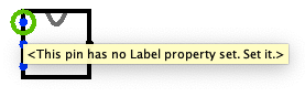
Once you have all the operations built, you can go back to the main circuit. Single-click on the ALU’s name on the left, and then you can place it onto the main circuit. There should be 3 pins on the left (for the inputs) and 1 on the right (for the output), like the image to the right.
If the pins (dots) are all on one side of the component, it’s because Logisim is very sensitive to the direction you have the input/output components facing in the component’s circuit. Inside the ALU component, select the ALU Out output and use the arrow keys on your keyboard to make it face the opposite direction. Now it should be on the right side of the box in the main circuit. This is why the output tool in the toolbar orients them that way when you first place them.
To be clear, this is what I mean about the directions of the inputs and outputs:

2.1 Are the inputs in the right order?
Remember, you aren’t allowed to move/reorder the tunnels on the main circuit. So the inputs on the left side have to be in the right order.

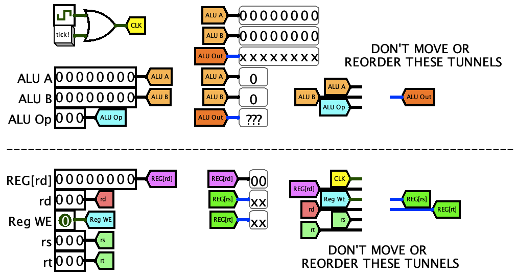
Put your mouse cursor over an input and you will see a green circle; then after a second, it will show the name of that pin. See the image to the right for what I mean.
From top to bottom, the inputs on the left side must be:
ABALUOp
If you get this message when you hover over a pin, then edit the ALU, click on the input/output components, and make sure their “Label” property is set. That is what is used to show you the pin label when you hover over it on the main circuit.
Attaching a tunnel to an input or output does not name it. You must set its “Label” property.
2.2 Testing the ALU
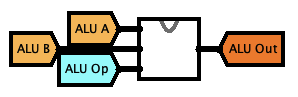
Finally, on the main circuit, drag the ALU in between the provided tunnels to hook up the inputs and outputs so it looks like the image to the right.
Now you can test it. For example, let’s test addition:
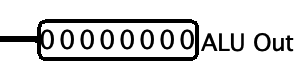
- On the main circuit, reset (Ctrl+R/⌘R). That sets the three ALU inputs to all 0s.
- Since an
ALUOpof000means addition, the ALU is already adding0 + 0. - The
ALU Outprobes should read00000000and0.- The top set of probes is set to binary.
- The bottom set of probes is set to unsigned decimal.
- Since an
- Use the hand tool to change the
ALU AandALU Binputs on the left, and watch what comes out ofALU Out.- It should be the sum of
ALU AandALU B.
- It should be the sum of
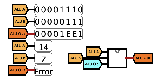
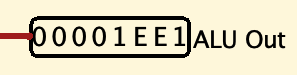
If there is a problem (e.g. a blue or red wire coming out of the ALU), see the section below. Otherwise, keep testing. Test all 8 operations to ensure they do what they should. These are the values for ALUOp and what they do.
000:A + B001:A - B- Check that
255 - 1(ALU A = 11111111,ALU B = 00000001,ALUOp = 001) outputs 254 (11111110). - If it outputs 253 (
11111101) instead, your adder’sc outoutput is incorrectly connected to your subtractor’sb ininput. Don’t put them right next to each other.
- Check that
010:A & B(the binary probes are the easiest to use to tell if this is working)011:A | B(same)100:A ^ B(same)101:~B(same - make sure it’s NOTing theBinput, and ignoresA!)110:A << B[2:0](values of B > 7 will be interpreted modulo 8 - a shift distance of 8 shifts by 0!)111:A >>> B[2:0](same)
Once you are satisfied all 8 operations are working correctly, you can move onto the register file.
Looking inside components
Let’s say you’re testing the ALU and you start getting a red or blue wire coming out of it. “Okay,” you say, “let’s look inside the ALU.” So you double-click its name on the left and…
Where’s the error? It looks fine. What? What’s going on?
See, when you double-click a circuit on the left side, what you are editing is kind of the “original template” of the circuit. You can think of it kind of like editing a class in Java.
But when you place that component in the main circuit, it makes an instance or copy of it, like using new in Java. And just like in Java, every time you make a new instance of the ALU, it has its own inputs, outputs, mux, adder, etc. etc. etc.
So to see where the red wire is coming from, you have to look inside the instance.

- use the hand tool
- click on the ALU component; a magnifying glass will appear
- double click the magnifying glass
Now you are looking inside the ALU instance. There is a message at the top of the screen (“You are viewing the state of an embedded subcircuit.”) to indicate this, and the background is also a yellowish color.
There’s the error! Now you can diagnose where the problem is coming from.
To go back to main, you can either:
- double click it on the left (which is fine cause there’s only 1
main); or - use ⌘← / Ctrl+Left-Arrow.
3. Making the Register File
Hey. Hey. The register file you are making is not exactly the same as what was shown in class. Please read the following paragraph. Thank you.
The register file is very similar to what was shown in class, but instead of 3 registers + a fake 0 register, it will have 7 registers + a fake 0 register. Also, the registers and the data input/outputs will all be 8 bits, not 32.
Time to repeat the process:
- Project > Add Circuit…, name it
Register Fileexactly. - Add its inputs and outputs like you did with the ALU.
- Inputs (note that this is the order they appear on the main circuit)
CLK- 1-bit clock signal (this is an input, not a clock component)REG[rd]- 8-bit value to be written tordifReg WEis 1Reg WE- 1-bit write enable input; enables writing to therdregisterrd- 3-bit number of register to be written to, ifReg WEis 1 (goes withREG[rd])rs- 3-bit number of the first register to read from (goes withREG[rs])rt- 3-bit number of the second register to read from (goes withREG[rt])
- Outputs
REG[rs]- 8-bit output of first register (selected byrs)REG[rt]- 8-bit output of second register (selected byrt)
- Inputs (note that this is the order they appear on the main circuit)
Now, using the circuitry provided in class as a template, you’ll build the register file yourself. Important notes:
- 👉👉YOUR REGISTER FILE WILL HAVE 8 (well, 7 + 1) REGISTERS, NOT 4 LIKE IN CLASS👈👈
- 👉👉YOUR REGISTER FILE WILL BE 8-BIT (REG[rd], REG[rs], REG[rt], and all registers)👈👈
- “Register 0” is not really a register, and can be represented as a
Wiring > Constantcomponent. - You can name the registers to make it easier to see which is which.
- Work on reading the values from registers first. That’s the pair of MUXes we saw in class.
- First, use the hand tool to poke the value of a register, and type in a new value. Do this to a few registers.
- Then, use the hand tool to poke the
rsandrtinput values, and see if the correct values flow out of the read MUXes (andREG[rs]andREG[rt]outputs).
- Then, work on writing the values to registers.
- 👉👉DON’T DUPLICATE THE REGISTERS THAT YOU ALREADY MADE. WRITE TO THE SAME REGISTERS YOU READ FROM.👈👈
- Don’t forget the clock signal input on every register.
- Also, don’t forget that “Register 0” is not really a register, so be careful which outputs of the demultiplexer connect to which registers!
- output 0 can be unconnected, that’s okay.
- output 1 goes to register 1, output 2 to register 2, etc…
- Last, be sure you are demultiplexing the
Reg WEinput, NOT theREG[rd]input! - You can test writing to a register by:
- setting the
REG[rd]input to the value you want to write (e.g.11110010) - choosing the register to write with
rd(something other than 0…) - setting
Reg WEto 1 - toggling the
CLKinput to simulate a clock cycle- the selected register’s value should change!
- setting the
Test your register file by poking the inputs some more. Here are some tests you can try (don’t reset between tests!):
- Put the value
1111 0000into register 1.- You should see its value change to
f0.
- You should see its value change to
- Put the value
0000 1101into register 2.- You should see its value change to
0d.
- You should see its value change to
- Read the values of registers 1 and 2 simultaneously (set
rsto 1 andrtto 2).- You should see
1111 0000(f0) coming out ofREG[rs]and0000 1101(0d) coming out ofREG[rt]. - If you only see
0000 1101(0d) coming out ofREG[rt], andREG[rs]is0000 0000(00),- make sure you didn’t reset between writing the two register values
- if you didn’t reset, then you have mistakenly demultiplexed the
REG[rd]input. You have to demultiplexReg WEinstead. Go look at your notes.
- You should see
- Make sure you can write to every single register.
- Put some value on
REG[rd], setReg WEto 1, setrdto001, toggle the clock input. Then changerdto010, toggle the clock input. Repeat until you’re sure you can write to every register.
- Put some value on
- Make sure that you can read from every single register, on BOTH outputs, in the RIGHT ORDER.
- Use the hand tool to click on register 1 and put
11in it; put22in register 2, etc. all the way to77in register 7. - Then change the
rsinput to read all 8 registers, and make sureREG[rs]is outputting the correct value for each register. - Repeat for
rt/REG[rt].
- Use the hand tool to click on register 1 and put
Finally, place it on the main circuit and test that it works when hooked up to the tunnels, too. (If you put your inputs in the wrong order in the Register File circuit, you might get orange wires and “Incompatible Width” errors.) Just remember that if you want to look at the values in the actual registers, use the hand tool to click on the component in the circuit, then double-click the magnifying glass.
By the way, the little semicircle at the top of the rectangle is not the clock input. It’s a decoration meant to be the little “orientation notch” that is seen on real chips to indicate which end is which. Like this. Awww. It’s cute.
Submitting
hrrrrnnghhh,,, , gradesopce…,,,,’