Your custom components look kinda dumpy by default. The pins are all cramped together, and they just look like featureless rectangles (with a little notch in the top, to make it look like a real computer chip, haha). But you can change it!
How to edit a circuit’s appearance
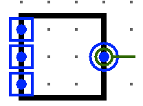
While editing a component’s circuitry, go to Project > Edit Circuit Appearance. For example, let’s say I’m editing a circuit with 3 inputs and 1 output. This is how it looks in the “Edit Circuit Appearance” window:

Wow, it’s really small. Just like on the circuit view, zoom in using the control in the bottom-left.

That’s better. Here’s what some of the symbols mean:
- The inputs here are on the left side, the blue squares with dots in them.
- The output here is on the right side, the blue circle with the dot in it.
- The green thing is the sort of “handle” where the component will rotate around if you change the direction it faces in the main circuit. Typically just having it on an output or something is fine, but you can technically put it anywhere you want.
Here’s what you can do with the arrow tool:
- Click and drag on an input or output to move it.
- It shows a mini-view of the circuitry in the bottom right so you can see which input/output it is, but for bigger circuits this is basically useless because the view is so small. idk man
- Edit shapes like the rectangle and notch by clicking on them.
- Drag them to move them around.
- Dragging the white box handles to change their shape.
- Edit their colors and other properties on the left.
- You can delete a shape while it’s selected. Bye bye notch!
The other tools along the top are pretty self-explanatory. It’s a mini art program. Whee!

My ALU is a bear, your argument is invalid.
Tips
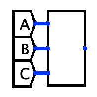
Don’t put the pins in the middle of, or outside, the component. It just looks weird and is hard to understand.
Put them on the sides where they make sense. The convention is for inputs to be on the left/bottom sides and outputs to be on the right/top sides.
Always make sure that all the sides of rectangles are “on the grid.” This avoids Problems. For example, these are both rectangles not aligned with the grid. See how you can see the gray dots next to the right side? That’s not good.
❌NO  BAD❌WRONG
  AAA❌
AAA❌
If they’re not aligned to the grid, it can cause issues with selecting and moving the component around on the main circuit.
Double-space your inputs and outputs if you want to be able to put tunnels into them side-by-side. Put them every other grid cell, like this:
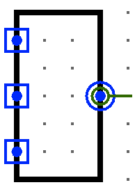
Now you can put tunnels into them right next to each other on the main circuit:
Be aware that if you move the pins around, you will have to reconnect them on the main circuit!